
In this paper, we attempt to present a new approach and analytical relation between perimeter-to-area ratio (P/A) and the plated thickness using Variable Area Window (VAW) test mask for improved thickness estimation. Although, the approach is illustrated using selective plating of gold films by varying two dimensional patterned windows on metallised silicon surface as an example, yet the method can be applied to other cases also. The method includes selective electroplating of gold in rectangular and circular windows wherein P/A of patterned shapes (squares, rectangles and circles) has been varied from 0.001 cm-1 to 0.4 cm-1 i.e. a factor of 400, a range normally used for practical modern MEMS devices. Experiments show that in general the thickness increases with increasing P/A because of current crowding. However, in contrast to using current density for control of this current crowding as reported in literature, we report that by careful design of mask pattern and improved material parameters, one can control and even achieve a slope reversal in the plot of thickness vs. P/A. The increase in thickness as measured by slope of linear fit is about 3 µm/(P/A in µm-1) for sharp edges compared to about 0.8 µm/(P/A in µm-1) for curved edges within the experimental errors. The general applicability of these relations to practical cases is confirmed by analysing the previously reported trends of data from the literature on Ni films using similar patterned shapes.
1. Introduction
A lot of MEMS sensors use gold films primarily for contact pads, transmission lines, pillars and bridges (RF devices), electrodes for capacitive accelerometers etc. because of its excellent stability and low electrical resistivity. Further, these films have high adhesive strength and ability for selective deposition on silicon. However, modern MEMS sensors demand ever shirking sizes down to say 5 µm x 5 µm or less. The thickness control and uniformity within a specimen of electroplated individual Gold plated microstructures in such small sizes is of utmost importance in MEMS device because many performance parameters are directly related to thickness[1-4]. Using conventional photolithography and electroplating, lot of MEMS sensors can be fabricated. However, one of the problems is to control and attain the same thickness of gold in varying patterned sizes which are required because of device design considerations. This directly affects the performance parameters. The usual one dimensional Farady’s equation is strictly not valid because of current crowding in small sizes particularly near edges. Very few authors have studied this problem. The thickness distribution across the wafer was studied by many authors [5-7]. It was found that the thickness profile follows a broad and shallow U-type curve radially across the wafer. The results were explained using varying voltage drop model from edge to the center. For patterned wafer plating, this non-uniformity in thickness has an effect not only on the thickness variation across a wafer but also on the thickness of the individual microstructures, which develop rabbit ears or nodule type cross-sectional profiles[8]. The ‘‘active-area density’’ model was developed to explain this behavior, that ascribed effect to current crowding at the edge of photoresist patterns [8].
However, a little attention has been paid to study and model the effects of varying window sizes on thickness that is encountered in modern MEMS sensors. The goal of the MEMS sensor designer is to have same thickness in each window irrespective of size. But this is not possible by physics because as the shapes become smaller and smaller due to demands of shrinking sensor sizes, the electric field lines become two dimensional in nature particularly near sharp edges, that leads to different current densities in different sizes and hence results in varying thickness in these shapes. The two or three dimensional analysis is cumbersome and difficult. Therefore, one needs to have some working relations so that variation can be estimated beforehand. In addition, proper tuning of design of shapes can be utilized to control this problem. Furthermore, the effect of varying process conditions on the profiles of microstructures and their uniformity across a wafer also has a role to play and is studied here. Since MEMS sensors require precise knowledge of plated thickness, we report an analytical relation for estimation of thickness using a Variable Area Window (VAW) mask that is used for selective area plating.
2. Experimental
A simple in house assembled system was used for plating. The Potassium Aurocyanate, K[Au(CN)2] salt procured from M/S Alfa Aesar was used. A solution was prepared by adding DI water. The pH value of the as-made plating solution was 5.5. Further, for improvement in thickness control for selective plating, for second set of experiments, grain refiner and make up salt were added with increased pH value of 6.0. The typical current density used was about 1 mA/cm2. A platinised titanium mesh type of electrode with 3-inch diameter was used as the anode. A magnetic stirrer was used to rotate and stir the solution at 250 rpm so that the concentration remains uniform and also removes bubbles from the sample surface. The plating temperature was kept constant at 23±1 °C. It was experimentally verified that when the current density was varied around the optimum range from 0.5-1 mA/cm2, although there was a change in the thickness, however, there is no appreciable change in the profile of the thickness distribution within a particular patterned of window (irrespective of the size) measured thickness. Most of the samples as reported in this study were prepared using the current density of ~1mA/cm2.
The specially designed mask as shown in Figure 1a (only a portion) was used to fabricate the samples with Gold deposition. The dimension of squares/rectangles was varied from a large size of 4000 µm x 4000 µm to 10 µm x 10 µm i.e P/A varies from 0.001 to 0.4 or by a factor of 400. Similarly for circles, the radius was varied from 5 µm to 4000 µm which yields a variation of P/A from 0.0005 to 0.4 µm-1. The Figure 1b shows the corresponding fabricated portion of the sample.
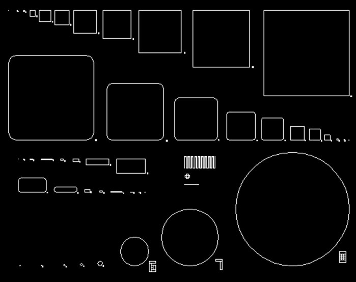
Fig. 1a: The layout of the portion of the mask showing many squares, rectangles and circles having varying areas
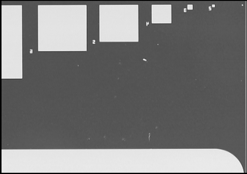
Fig. 1b: The portion of the fabricated sample showing patterned electroplated squares, rectangles and circles having varying areas.
Silicon samples were cleaned by standard RCA procedure. Briefly it uses TCE, Acetone, DI water (ultrasonic bath) HF dip etc. and was then rinsed in de-ionized water. Using a RF/DC Sputtering system, a seed layer of 130 nm was deposited on a Si-wafer. The seed layer was then coated with 6.5 µm thick layer of photoresist (PR) MAP 1275. Baking of PR was done at 90 °C for 30 min in a convection oven. Further, the UV exposure was done using an Karl Suss mask aligner model MJB 3. Usual developing and rinsing steps were followed. Immediately after electroplating, the PR was removed by immersing the samples in acetone.
The electroplated thicknesses of the patterned shapes were measured using a DekTak profiler, which has a resolution of 20-30 nm.
3. Results and Discussions
Initial preliminary thickness was estimated using a simple one-dimensional Faraday’s formula:
Equation 1:
T = (I*t*W*10000)/(n*F*rho*S)
Where:
T = thickness in microns, I = current in coulombs per second, t = time in seconds, W = atomic weight of the metal in grams per mole, n = valence of the dissolved metal in solution in equivalents per mole, F = Faraday’s constant in coulombs per equivalent. F = 96,485.309 coulombs/equivalent, rho = density in grams per cubic centimetre, S = surface area of the plated part in square centimetres, 10000 is a multiplicative constant to convert centimeters to microns.
Since the thickness is proportional to the current density, a thicker film is expected to be deposited on the edge of a wide (i.e. low P/A) patterned structure (square, rectangle or circle) due to the increased current density, whereas a thinner film is expected in the middle of the structure. As the microstructure becomes narrower (i.e. high P/A), the current crowding becomes more severe across the whole width of the patterned microstructure. Due to this, the effective current density becomes much higher than that in the wide structure. This leads to a thicker film for a narrow microstructure as was shown by Lo et al [8] for a different case of Ni selective films.
Figure 2a shows the plot of P/A vs. thickness wherein we can see that as expected, the thickness increases with increasing P/A barring one exception in case of square pattern, that shows a -ve peak i.e. a minima at P/A of about 2.7e-3 cm-1. Initially, it was thought to be measurement error or artefact, but repeat of the experiment with different solution again showed this minima at almost the same value of P/A. Further, it may be seen from this figure that in case of circles we get a smaller variation in thickness i.e. smallest slope (assuming linear behaviour) compared to rectangular patterns having sharp edges which are prone to current crowding. The phenomena of increasing thickness was also earlier observed by Lo et al [8], although their main focus was to study the effect of current density on magnitude of rabbit ear at the edges of the patterned square shapes. They found that the thickness profiles within the patterned windows strongly depend on the process conditions. They reported that for an optimal plating current density, the microstructure has a rabbit-ears profile and the thickness of a narrow microstructure is thicker than that of wide ones. For their case of J=30 mA/cm2, thickness increased by approximately 14 % when P/A was increased by a factor of 100 (Figure 1a of Ref.[8]). This is a similar trend as was measured by us and is expected as per simple one dimensional analysis. However, further they found that at a lower current density of 4 mA/cm2, the microstructure has a cap-like cross-sectional profile, and a narrow structure is thinner than wide ones. Their value in thinner window decreased by about 20% when P/A increased by about a factor of 13.3 (Figure 1c of Ref.[8]). That means the thickness in narrow patterns i.e high P/A shows a lesser value in contrast to expectation. Intermediate values were obtained in intermediate value of P/A. Further they showed amplitude of rabbit ear formation i.e. excess thickness formation at the edges particularly in patterns with high P/A could be reversed with decreasing current density. Based on their observations, we can infer that for our case of square patterns having P/A of 2.7E-3 cm-1 or lower there is anti-current crowding, which means that area is big enough and the optimal current density is not optimal for such an large area. As for the case of rectangular pattern, this -ve peak or minima may be occurring at further lower values of P/A.
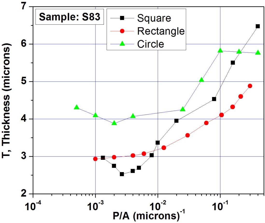
Fig. 2a: The Plot of perimeter to area ratio (P/A) of patterned shapes versus thickness in the centre of the pattern
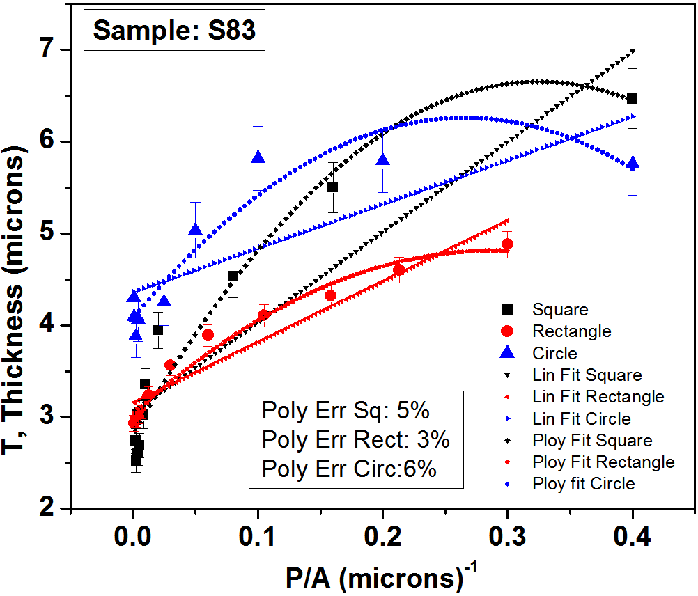
Fig. 2b: The Plot of perimeter to area ratio (P/A) of patterned shapes versus thickness in the centre of the pattern. The linear and polynomial fit to the data for each case has also been shown.
Next we tried to fit the analytical relations (linear and non-linear) between P/A vs. thickness, which would be directly useful to us and the workers in the field. Figure 2b shows the plot of P/A vs. thickness along with linear fit and second degree polynomial fit. One can see from this figure that for all the cases the trend is that with P/A increasing from ~0.0005 µm-1 to 0.45 90 °C µm-1, the thickness increases from 2.5 µm to 6.5 µm. In addition, it may be seen that in case of square or rectangle patterns, the curves have same intercept of about 3 um within experimental error on Y-axis for very low values of P/A. This is expected because large size squares or rectangles should not differ much in the expected thicknesses. This value of near zero intercept can be taken to be representative of true one-dimensional case valid for large size geometries or patterns, wherein increase in thickness due to 2-D current crowding effects are minimal. However, as regards circle pattern, this intercept on Y-axis for low value of P/A is about 4µm i.e. almost one micron in excess compared to rectangular geometry. This is explained by the fact that in case of circular geometry we have minimal edge effects and field lines are expected to be more uniform and having circular symmetry resulting in increased current density yielding a higher thickness. This can be a valuable tool in the hands of designer wherein simply by making the round edges, one can tailor the thickness variation within the varying size of patterns to a minimum. This will be discussed further later while discussing effect of rounded corners for rectangular geometries.
Thus depending on the variation in dimensions of pattern sizes within a die, one can estimate the expected increase in thickness for smaller patterns having high P/A ratio using the slope of the simple linear fit. In our case this fit is accurate within 15 % as per our analysis. Although the data indeed follows the trend of increasing T with increase in P/A, however, the close examination reveals that for all the three cases of square, rectangle and circle, clearly the experimental data does not seem to follow linear trend properly. The linear fit relations for geometries like squares, rectangles and circles are as follows:
Equation 2.1:
T(Square)=3.04797+9.83749*(P/A)
Equation 2.2:
T(Rectangle)=3.15195+6.62579*(P/A)
Equation 2.3:
T(Circle)=4.36054+4.78608*(P/A)
As shown by the error bar margins (Figure 2b) the estimated error of linear fit was ~15 % particularly for high P/A range of 0.3 to 0.4 cm-1. This is attributed to two-dimensional nature of field and current crowding at the edges. In short we can state that within experimental errors, the increase in thickness as measured by slope is about 10 µm/(P/A in µm-1). This can be very handy and useful relation for the workers in the field.
Next we tried to fit the same data using a simple second degree polynomial which yielded more accurate fit to the data as follows:
Equation 2.4:
T(Square) =2.8156+23.65*(P/A)-36.43*(P/A)2
Equation 2.5:
T(Rectangle) =3.03186+12.31113*(P/A)-21.27519*(P/A)2
Equation 2.6:
T(Circle) =4.08145+16.40912*(P/A)-30.88595*(P/A)2
It may be seen from Figure 2b that compared to linear fit wherein maximum fitting error was 15 %, the error is reduced to 5 % for Square, 3 % for Rectangle & 6 % for Circle using second degree polynomial fit. The second term in equation. (2.4) to (2.6) can be assumed due to contributions because of two-dimensional nature of filed lines.
The above fitted linear and non-linear relations are valid for a fixed current density for selective plating gold films using materials as described in section 2 but the approach can be applied to other metallic films also. The idea is to present a simple relation for designers to assess the impact of thickness due to increasing P/A. One can further optimize or improve by other process parameters as will be shown next. Such an approach can be utilized while building a pdk (process development kit) for the foundry that is utilized by the designers.
To verify the trends of the results and further reduce the effects of increasing T at high P/A, we repeated the experiment and fabricated another batch wherein we prepared a fresh solution having a higher conductivity and with added grain refiner that is expected to yield better thickness control within a die or within a wafer. It may be mentioned that without these additives the conductivity was 5-6 mS/cm which became 70-72 mS/cm after addition of additives. Specifically the comparison of sharp edges to rounded edge was studied as was discussed in earlier paragraph.
Figures 3a-b show the data for all the three cases of square, rectangle and circle, along with linear fit and polynomial fit. Clearly, it may be seen that the experimental data does follow the similar trends as in Figure 2a. Assuming a linear fit, we get the slopes and intercepts as shown in equations below:
Equation 3.1:
T(Square)=3.417+2.05806*(P/A)
Equation 3.2:
T(Rectangle)=3.43873+1.81907*(P/A)
Equation 3.3:
T(Circle)=3.82866+1.12469*(P/A)

Fig. 3a: The Plot of perimeter to area ratio (P/A) of patterned shapes versus thickness in the centre of the pattern.
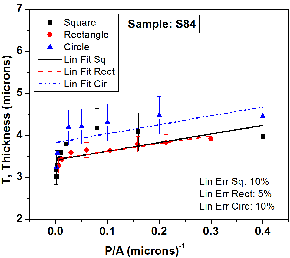
Fig. 3b: The Plot of perimeter to area ratio (P/A) of patterned shapes versus thickness in the centre of the pattern. The linear fit to the data for each case has also been shown.
The maximum linear fit errors is 10 % for square (barring one point showing minima at P/A of 2.6e-3 µm-1), 5 % for rectangle and 10 % for circle which is 5 % lower compared to earlier case of Figure 2b. As can be seen from this figure, we have been able to reduce the P/A effect by 5 % by combined effect of improved materials.
Next in another sample, we tried to specifically compare the effect of rounded edges on the slopes of P/A vs. T curves as shown in Figures 4a-b. As can be clearly seen from Figure 4b, the slope of round edge is reduced to considerably compared to un-rounded edges and we could even reverse this slope.
The above result is a new approach to achieve thickness control due to current crowding in high P/A geometries. Earlier, Luo [8] et al. obtained such control using current density changes which requires large experimentation for optimization. However, using our approach it produces inherent uniform electric field lines which are in general desirable for semiconductor device operations. Due to rounded edges we have circular symmetry in filed lines.
Actual linear fitted values of slopes are as follows:
Equation 4.1:
T(Square with sharp edges)=3.21158+3.11906*(P/A)
Equation 4.2:
T(Square with curved edges)=3.87056-0.80026*(P/A)
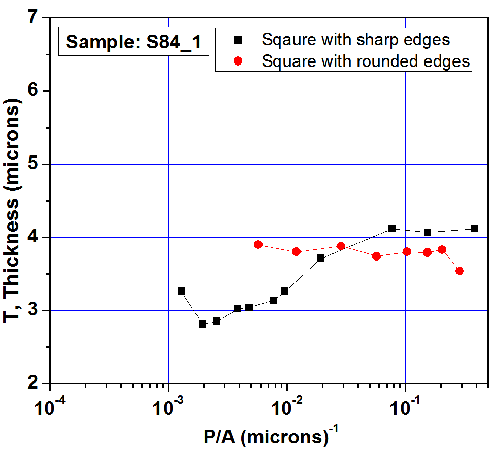
Fig. 4a: Comparison plots of perimeter to area ratio (P/A) versus thickness between square with sharp edges and with curved edges.
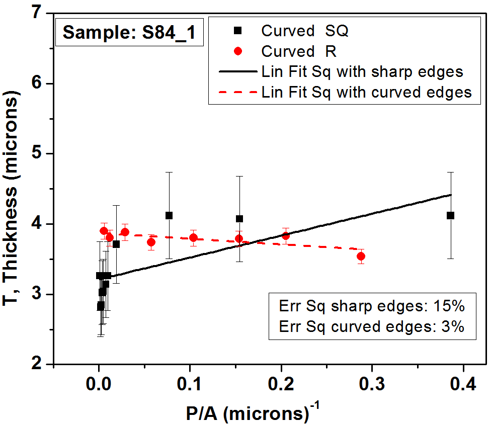
Fig. 4b: The Plot of perimeter to area ratio (P/A) of patterned shapes having curved edges versus thickness in the centre of the pattern. The linear fit to the data for each case has also been shown.
In this case we can see that within experimental errors, the increase in thickness as measured by slope is about 3 µm/(P/A in µm-1) for sharp edges compared to about 0.8 µm/(P/A in µm-1) for curved edges. These type of relations can be utilized designers as applicable to their laboratories. In short we can state that one can control the effect varying P/A on thickness down to 3 % by improved material and careful design wherein sharp edges could be changed to rounded edges.
4. Conclusions
In conclusion, we have presented a new simple analytical approach for improved thickness estimation and control in pattern selective plating. Further, in contrast to using current density for control of current crowding as reported in literature, we report that by careful design of mask pattern and improved material parameters, one can control and even achieve a slope reversal in the plot of thickness vs. P/A. A novel and simple linear one dimensional and second degree polynomial relations have been developed for estimation of gold microstructure thickness on Silicon wafers which is rather simple, inexpensive and advantageous. It requires only a simple one mask and short fabrication time, a small instrumental input and can be operated in batches and so this process may be applied in the microelectronics industry while developing a pdk (process development kit) for foundry services.
Acknowledgements
The authors would like to thank Director, Solid State Physics Laboratory for his continuous support and for the permission to publish this work. Help from other colleagues of PLG team is also acknowledged.
References
- MEMS Materials and Processes Handbook, Eds. Reza Ghodssi and Penyen Lin, Springer, New York, (2010).
- T. A. Green, M. J. Liew, and S. Roy, J. Electrochem. Soc., 150, pp. 104-110, (2003).
- J. W. Judy, R. S. Muller, and H. H. Zappe, J. Microelectromech. Syst., 4(4), pp. 162-169, (1995).
- J. C. Sadak and F. K. Sautter, J. Vac. Sci. Technol., 11, pp. 771-776, (1974).
- K. M. Takahashi, J. Electrochem. Soc., 147(4), pp. 1414-1417, (2000).
- J. Flake, Y. Solomentsev, J. Cooper, and K. Cooper, J. Electrochem. Soc., 150, pp. C195-C201, (2003).
- S. Mehdizadeh, J. O. Dukovic, P. C. Andricacos, L. T. Romankiw and H.Y. Cheh, J. Electrochem. Soc., 139, pp.78-91, (1992).
- J. K. Luo, D. P. Chu, A. J. Flewitt, S. M. Spearing, N. A. Fleck, and W. I. Milne, Journal of The Electrochemical Society, 152, pp. C36-C41, (2005)
PDF Version of the article |
Flash Version of the article |
|
| [qr-code size=”2″] | ||