Nickel-alumina composite films were obtained by electrocodeposition using different deposition techniques, viz. direct current (DC) deposition and pulse-reverse plating (PRP). Particle incorporation was determined by means of energy-dispersive X-ray spectroscopy and glow discharge optical emission spectrometry (GD-OES). The structure of the films was analyzed using electron microscopy, viz. scanning electron microscopy (SEM), electron backscatter diffraction (EBSD), transmission electron microscopy (TEM), and X-ray diffraction. A <100> fiber texture was found for pure nickel films, which was reduced due to a change in plating conditions and particle incorporation. EBSD mappings indicate that the nanosized particles inhibit nickel growth and thus lead to a smaller nickel crystallite size combined with a distinct loss of the <100> texture. Scanning transmission electron microscopy (STEM) and TEM reveal that the inclusion of alumina nanoparticles preferentially takes place in the grain boundary region where the particles terminate the growth of nickel. High-resolution TEM imaging proves a complete embedding of nanoparticles by the nickel matrix without any voids.
1 Introduction
Metal-matrix composite films can be obtained by electrocodeposition (ECD), i.e., particle incorporation during metal deposition from electrolytes containing a dispersion of ultra fine particles [1]. Depending on the combination of matrix and dispersed phase, coatings produced may have unique chemical, electrical, and mechanical properties [2–5]. Recently, ECD has been proposed as a technique for producing abrasionand corrosion-resistant coatings for automotive and aerospace applications [6]. Moreover, a variety of nanoparticles such as Al2O3 [7], C [8, 9], SiO2 [10, 11], ZrO2 [12, 13], and SiC [14–17] have been successfully codeposited with several metals, e.g., Cu, Co, Cr, Au, Ni, and Ag, for use in electrocatalysis, wear and corrosion protection, dispersion strengthening, and lubrication of surfaces [6, 18, 19]. Properties of composite coatings depend significantly on their composition and structure [20]. Uniform distribution and high amounts of codeposited particles within the metal matrix have been found to be crucial for improving coating properties [21, 22]. In many cases, the enhanced performance of the coatings is caused mainly by a change in microstructure of the metal matrix [15, 22] and not so much by the presence of the particles themselves. However, no characterization of the metal-particle interface was performed in the quoted references.
Since structure and properties are crucial for utilization of any material, characterizing these properties is a very relevant issue in composite film development [23]. In previous work [22, 24, 25], we discussed the effect of certain deposition parameters on composition as well as structure and properties of Ni-Al2O3 composite films prepared by means of direct current (DC) and pulse-reverse plating (PRP). Nickel was chosen as matrix material since it is a common industrial metal for decorative and functional coatings. The overall objective of this work was to systematically investigate the composition and structure of selected composite films by electron microscopy (QBSD, STEM, TEM, EBSD), X-ray diffraction, and spectroscopic procedures (GD-OES). While X-ray diffraction yields information from a relatively large volume of a sample, electron microscopy probes cover a rather confined volume. Hence, both methods are important for an in-depth microstructural characterization of deposited composite films.
2 Experimental Procedure
ECD experiments were carried out using an acidic nickel sulphamate electrolyte containing 1.08 M Ni(NH2SO3)2, 0.04 M NiCl2×6H2O, and 0.65 M H3BO3. Commercially available alumina nanoparticles used for the codeposition experiments had a primary particle size of 13 nm as specified by the supplier (Aeroxide Alu C, Degussa). Particle content of the electrolyte varied from 0 to 10 g/l. The pH-value of the electrolyte was measured before and after each experiment and, if necessary, adjusted to pH 4.3. Temperature was maintained at 40 °C with a Haake thermostat (G D1, accuracy ±1 °C) and the solution was mechanically stirred (250 rpm) using a magnetic stirrer. Substrates were copper disks with an electroactive area of 0.22 cm2. They were ground with 4000 grit silicon carbide paper, ultrasonically cleaned in acetone, cathodically degreased in alkaline solution (UNAR EL 63, Schering), and activated with Uniclean 675 solution (Atotech Germany). Direct current (DC) deposition was carried out with a current density between 1 and 10 A/dm2. In the PRP experiments, pulse on-time (ton) was varied between 50 and 400 ms and reverse-pulse time (trev) was kept constant at 20 ms. The cathodic peak current density (ip) was 5 A/dm2 whereas anodic peak current density (ian) was either 1 or 5 A/dm2. After electrodeposition, the samples were sonicated in distilled water for 10 minutes to remove loosely adhering particles. For further details on experimental setup and plating conditions see Ref. [24].
The depth profile of film composition was determined by means of GD-OES using a GDS 750 (Spectruma Analytik, Germany). The system was calibrated using standard reference materials, i.e., pure nickel and nickel alloys (IARM, Analytical Reference Materials International, USA). Finally, raw intensity versus time data were converted to elemental concentrations versus depth.
X-ray diffractograms were recorded with a scan rate of 0.12° min–1 for two-theta ranging from 10 to 100° (XRD, Siemens D5000). The size of the nickel crystallites was determined from the broadening of the (200) and/or (111) reflections according to the Debye-Scherrer equation [26].
A Fesem Neon40EsB (Zeiss, Germany) was used at 25 kV with a scanning transmission electron microscopy (STEM) detector as well as an EBSD camera (EDAX TSL, USA). EBSD maps were calculated after a minor clean-up, excluding grain dilatation but comprising grain confidence index (CI) standardization with 2° tolerance angle and neighbor CI correlation, and they show the correctly indexed fraction with CI > 0.1.
For backscattered secondary electron (BSE) imaging, voltage was lowered to 10 and 5 kV. Cross-sections were prepared with a final oxide polish (OP). For TEM, the composite films were mechanically separated from the substrate. Disks of 3 mm in diameter were cut and ion-polished until electron transparency using 3 kV Ar ions with 6° incidence angle. Ion polishing was performed on both sides. The utilized TEM (Hitachi 8110) was equipped with an LaB6 cathode and was operated at 200 kV, which enables imaging in high resolution complemented with diffraction patterns, bright (BF) and dark field (DF) imaging.
3 Results and Discussion
3.1 Particle Incorporation Analysis
One goal of our research was to systematically investigate the effects of a variety of process parameters on the amount of particle incorporation during ECD of Ni-Al2O3 composites. Detailed results can be found in Refs. [22, 24], a summary is presented below.
In DC depositions, particle incorporation in the nickel matrix ranged from 0 to 4.4 percent by volume Al2O3. Low values of current density were found to improve nanoparticle codeposition. A maximum incorporation of approximately 4.4 percent by volume Al2O3 was obtained at a current density of 1 A/dm2 and a particle content of 1 g/l [22].
GD-OES analyses were undertaken to validate the incorporation results determined by EDX measurements [22]. Figure 1 compares the amount of particles in the nickel layer obtained with these two techniques. Although GD-OES incorporation results are obviously lower than those determined by EDX analysis (Fig. 1a), the overall trend with a change in particle content of the electrolyte is similar, i.e., the highest amount of particles in the layer is confirmed at a particle content of the electrolyte of 1 g/l Al2O3. Additionally, GD-OES analyses emphasize an overall uniform particle distribution within the metal matrix (Fig. 1b). The differences in the results of both methods, EDX and GD-OES, can be explained by the fact that a quantitative GD-OES analysis of film composition is based on a calibration with an appropriate reference material. Calibration of GD-OES was achieved using pure nickel and nickel alloys as reference materials. Furthermore, differences in the incorporation results can also be attributed to differences in the size of the area analyzed [27]. While the area of analysis is limited to a few hundred μm2 in the case of EDX, GD-OES probes a larger volume of the composite film.
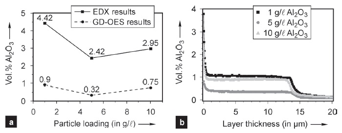 Fig. 1: Al2O3 content in nickel films plated at a current density of 1 A/dm2 from an acidic sulphamate electrolyte containing various concentrations of Al2O3 nanoparticles; (a) particle content determined by EDX (squares) [22] and GD-OES (circles); (b) GD-OES depth profiles of nanoparticle distribution in the film (dark squares: 1 g/l Al2O3, grey circles: 5 g/l Al2O3, light-grey triangles: 10 g/l Al2O3)
Based on the results of DC plating, PRP conditions were optimized in order to achieve compact nickel surface finishing with a smooth surface morphology. Particle incorporation measured by EDX ranged from 2.7 to 10.7 percent by volume alumina, depending on PRP conditions. The maximum incorporation during PRP, i.e., 10.7 percent by volume Al2O3 in nickel, is found at a cathodic pulse length of 400 ms, a cathodic peak current density of 5 A/dm2, an anodic pulse length of 20 ms, and an anodic peak current density of approximately 1 A/dm2 [24]. In general, incorporation of 13 nm Al2O3 particles is enhanced by longer cathodic pulse times as well as lower anodic peak current densities.
3.2 Nickel Matrix Characterization
Table 1 summarizes the grain features derived from XRD and EBSD studies. X-ray diffraction was used to identify the texture and crystallite size of the nickel matrix. XRD patterns of pure nickel deposits prepared by DC deposition reveal a strong (100) preferred crystalline orientation [28, 29] detected by the intense (200) reflection. The quality of the <100> fiber texture is significantly affected by the working parameters, i.e., current modulation and particle loading of the electrolyte. Due to the application of PRP conditions as well as the codeposition of alumina nanoparticles, a loss of texture appeared, reflected by the reduction of the (200) line and the relative enhancement of the (111), (220), and (311) lines [29]. These results were confirmed by the EBSD studies.
Tab. 1: Grain features of nickel matrix in electrodeposited films; deposition conditions: DC: I = 10 A/dm2; PRP: iP = 5 A/dm2, ton = 400 ms, and ian =1 A/dm2, trev = 20 ms; composites plated from electrolyte containing 10 g/l 13 nm Al2O3 nanoparticles

The crystallite size of the nickel films was estimated from diffraction line broadening using the Debye-Scherrer method [26] as well as EBSD analysis (Tab. 1). Typically, EBSD is a technique used for microstructural characterization in materials science [30, 31]. Compared to X-ray diffraction experiments, which yield wide-ranging texture information of the whole film, EBSD illustrates local details of crystal growth on the micron scale [32]. Thus, the technique is advantageous in studying metal growth at the nickel-substrate interface as well as around codeposited nanoparticles. Mean grain size parameters are derived from EBSD quality maps collected from the lower part of the layer near the substrate as well as at the film surface. Twin boundaries are identified and excluded from grain size evaluation.
Gain sizes determined by EBSD measurements are obviously larger compared to those computed from XRD patterns (Tab. 1). Differences might be caused by the fact that polycrystalline samples rather often include dislocations, stacking faults, twin planes, and further lattice defects which hamper interpretation of the XRD peak broadening. In particular, crystallite sizes determined by XRD analysis reflect the size of coherently diffracting domains [23]. In general, this value is lower than the grain size obtained by electron microscopy [23]. Furthermore, values derived from XRD comprise grains below 100 nm in contrast to EBSD results due to the scanning-step size. Hence, it has to be specified which experimental technique is used for determining crystallite/grain size in order to allow any comparison. Nevertheless, both values show the same tendency. In the case of PRP, a crystallite size development unexpected at first glance is observed. As a result of particle codeposition, nickel crystallite sizes show a tendency to increase which can be explained by the insulating nature of alumina nanoparticles. Owing to particle incorporation, the electroactive area of the electrode decreases, which finally leads to a local increase in current density. The effect of current density on the properties of nanocrystalline nickel plated from sulphamate electrolyte is described in Ref. [33]; increasing crystallite sizes are found with increasing current density.
As discussed in detail in Section 3.3, the films consist of a fine-grained initial layer without particles and a subsequent layer showing columnar crystal growth. This is why grain size distribution is not unimodal and a number of grains are significantly larger than the average grain size shown in Table 1. PRP deposition yields higher mean grain sizes whereas particle incorporation causes lower mean grain sizes. The mean aspect ratio of the columnar grains is about 2. High-angle boundaries (> 15°) include about 24 percent of twin boundaries. Low-angle boundaries (< 15°) comprise a rising percentage of the total boundary length from 20 percent for pure nickel to 22 percent for the composite matrix.
3.3 Particle Incorporation Behavior – Distribution and Bonding to the Matrix
Material properties of composite films depend mainly on particle distribution, their bonding to the matrix, and their influence on the microstructure of the metal matrix. In the following, electron microscopy results will be discussed for two selected composite samples prepared from a sulphamate bath containing 10 g/l Al2O3 particles using either DC or PRP.
Images were obtained by backscattered electrons using a quadrant detector (QBSD). This is an annular diode detector divided into four equal sized sections which can be treated as four separate BSED detectors with various mixing of their outputs. If the outputs are simply added in so-called compositional mode, images proved to be an appropriate tool for visualizing nickel crystal growth by means of orientation contrast as well as for particle distribution by means of material contrast.

Fig. 2: QBSD image (a) and IPF color-coded nickel map (b) of pure nickel film deposited from sulphamate electrolyte by PRP: ip = 5 A/dm2, ton = 400 ms, and ian = 1 A/dm2, trev = 20 ms
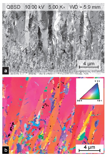
Fig. 3: QBSD image (a) and IPF color-coded nickel map (b) of Ni-Al2O3 film deposited by PRP (same plating conditions as for Fig. 2, 10 g/l 13 nm Al2O3 in electrolyte)
The QBSD image taken from a sample prepared by PRP (Fig. 2a) confirms field-oriented growth of nickel films from sulphamate bath as detected by XRD [29] and EBSD. A distinct <100> fiber texture in growth direction is illustrated in the nickel crystal orientation map color-coded by the inverse pole figure (IPF) (Fig. 2b). Layer growth direction is upwards in all cases. Starting with a nearly one micron thick and fine initial crystalline layer, the subsequent layer is formed by columnar grains with increasing size from approximately 0.4 μm inside the film to about 1.1 μm at the film’s surface. The formation of an initial layer with tiny grains in the vicinity of the substrate has been previously reported for nickel and nickel composites plated from an acidic Watts electrolyte [32]. The effect of alumina nanoparticle incorporation on grain growth of the nickel matrix as well as a good indication of particle distribution in the metal matrix can be derived from the QBSD images shown in Figures 3a and 4a. Alumina particles, mainly present in the form of agglomerates, appear as dark spots in the lighter nickel matrix. Using EDX analysis in the crosssection, the volume fraction of alumina particles in these films was determined to be approximately 11 percent by volume (PRP sample, Fig. 3) and approximately 2.5 percent by volume (DC sample, Fig. 4). In good agreement with pure nickel film (Fig. 2a) and findings in Ref. [32], the composite film formation starts with an initial layer of tiny grains adjacent to the substrate. With increasing distance from the substrate, columnar nickel grains appear. However, these columnar nickel grains seem to be refined due to the presence of particles (Figs. 3a and 4a).
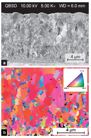
Fig. 4: QBSD image (a) and IPF color-coded nickel map (b) of Ni-Al2O3 film deposited from sulphamate electrolyte containing 10 g/l 13 nm Al2O3, DC: i = 10 A/dm2
Regardless of the current modulation used, black spots in the color-coded nickel maps of composite films (Figs. 3b and 4b) represent highly disordered parts of nickel matrix probably caused by alumina particle incorporation. Although there is a certain ambiguity in this interpretation, further proof of the localization of alumina particles comes from nickel and alumina orientation maps taken at a reduced step size of 50 nm. The image quality map (Fig. 5a) represents low-ordered regions in the sample, i.e., nickel grain boundaries and dark spots near grain boundaries as well as in the middle of the central grain. Few are visible in the orientation maps of nickel (Fig. 5b) and of alumina (Fig. 5c). Nevertheless, no alumina was detected by EBSD analysis in the central grain where the image quality map (Fig. 5a) suggests incorporated particles. We would like to note that this finding does not prove the absence of particles, but rather has to be attributed to the resolution limits of EBSD compared with particle size. In conclusion, both QBSD and EBSD maps indicate that alumina nanoparticles are predominantly incorporated in the grain boundary zone. It is apparent that alumina particles terminate the columnar nickel crystals and consequently affect the direction of growth which is consistent with XRD results [29].
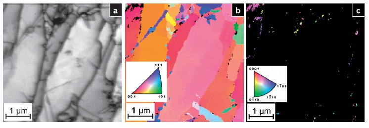
Fig. 5: Detail of Fig. 3 in image quality map (a), IPF color-coded nickel map (b) and IPF color-coded alumina map (c)
Furthermore, the detailed incorporation behavior of alumina particles, i.e., agglomerate size and distribution of codeposited particles in the nickel matrix as well as particle-nickel bonding, was studied using SE, STEM, and TEM imaging. Results will be discussed in the following for the composite film plated by PRP. The resolution in backscattered electron imaging is limited by their relatively high escape depth. Resolution can be enhanced using secondary electrons (Figs. 6a, b). In SE imaging, alumina particles appear as dark spots. In addition, the images reveal twins and fine twin lamellae in the nickel grains. Imaging of electron transparent samples with STEM allows higher magnification. In dark field imaging, particles appear as black and dark grey spots in the vicinity of small grains (Fig. 6c). Grain refinement by particle incorporation is striking but lower compared to the grain refinement in the initial layer (Fig. 6d). Codeposited particles provide new nucleation sites similar to the conditions at the substrate interface, although not in the same multitude. However, grain refinement by particle incorporation is lower than in the interface region.
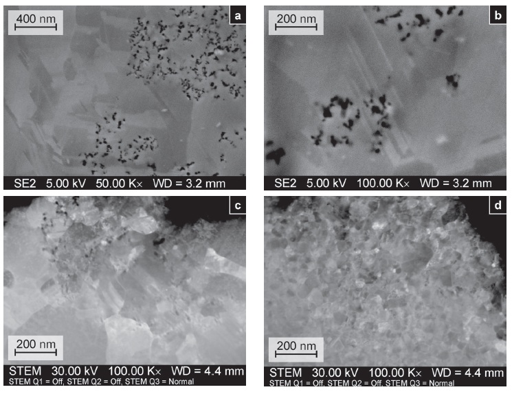
Fig. 6: SE (a, b) and STEM (c) images of Al2O3 particles in Ni matrix deposited by PRP (same plating conditions as for Fig. 2), STEM image (d) of initial layer for comparison
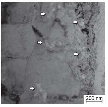
Fig. 7: TEM image of Ni-Al2O3 film produced by PRP (same plating conditions as for Fig. 2, 10 g/l 13 nm Al2O3 in electrolyte, white arrows indicating selected codeposited particles)
Nevertheless, resolution in SE imaging is insufficient for studying the particle-metal interface. Transmission electron microscopy bright field imaging shows numerous chains of agglomerated alumina particles, and sometimes, single particles in the polycrystalline matrix as bright spots in bright field imaging (Fig. 7, white arrows marking selected particles). The alumina nanoparticles are produced by the Aerosil® process which essentially is a high-temperature hydrolysis of particular gaseous metal chlorides [34]. The chain-like agglomeration observed in the nickel matrix already originates in the cooling process during particle preparation and was confirmed by the supplier. At higher magnifications, incorporated individual particles are characterized by a nearly spherical shape and a size of about 10 to 30 nm. The two coalescent particles in Figure 8 show adjacent lattice planes. Additionally, twin lamellae in the metal matrix, nickel lattice planes, and moiré patterns indicating low angle rotation boundaries are observed by high resolution imaging. The interface between the matrix and the particles suggests proper particle-matrix bonding without any voids.
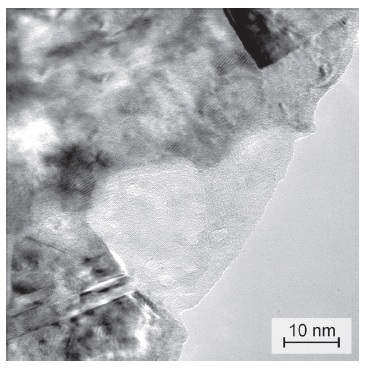
Fig. 8: High-resolution TEM image of Ni-Al2O3 film (same plating conditions as for Fig. 2, 10 g/l 13 nm Al2O3 in electrolyte) demonstrating the incorporation of two conjoined Al2O3 particles
In summary, our electron-microscopic studies have revealed that both agglomerated as well as individual alumina particles are incorporated preferentially near grain boundaries. Finally, it has to be emphasized that in the case of both DC deposition and PRP, particles appear to be codeposited as individual particles as well as in agglomerates with sizes of about 200 nm, which is in perfect agreement with our previous results [22, 24].
4 Summary
Nickel alumina composites were prepared by means of electrocodeposition using DC and PRP deposition. The structure of composite films was analyzed using a combination of electron microscopy and X-ray diffraction techniques.
A strong <100> preferred orientation is found for pure nickel film deposited from sulphamate bath, which was reduced due to a change in plating conditions and particle incorporation. Nanosized alumina particles are found to inhibit nickel growth and thus lead to smaller crystallite size combined with a distinct loss in texture.
A preferred particle inclusion in the grain boundary zone was suggested by EBSD mapping of the nickel matrix and confirmed by TEM. Hence, codeposited particles seem to terminate nickel growth. Highresolution TEM imaging of nanocomposites confirm the incorporation of alumina nanoparticles in nickel matrix without any voids. Particle incorporation appeared as chains of particles. Even though particle concentration increased in PRP, we found no evidence for differences in particle agglomeration when comparing PRP and DC composite layers. Further work is necessary in order to achieve more homogenous particle incorporation.
Acknowledgments
This work was financially supported by the Deutsche Forschungsgemeinschaft (DFG) (Grant BU 1200/10-1 and BU 1200/14-1). Alumina particles (Aeroxide Alu C) were provided as free samples by Evonik Degussa GmbH, Germany. A. Bund gratefully acknowledges support from the DFG in form of a Heisenberg Fellowship.
References
- J. B. Talbot: Plat. Surf. Finish. 91 (2004), 60
- E. W. Brooman: Galvanotechnik (2006), 58
- L. Shi, C. Sun, P. Gao, F. Zhou, W. Liu: Appl. Surf. Sci. 252 (2006), 3812
- N. S. Qu, D. Zhu, K. C. Chan: Scripta Mater. 54 (2006), 1421
- E. Brooman: Plat. Surf. Finish. 94 (2007), 38
- J.-P. Celis, J. Fransaer: Galvanotechnik 88 (1997), 2229
- J. L. Stojak, J. Fransaer, J. B. Talbot: Review of Electrocodeposition; in: R. C. Alkire, D. M. Kolb (Eds.): Adv. Electrochem. Sci. Eng., Weinheim: Wiley-VCH, 2002
- B. Bozzini, G. Giovannelli, P. L. Cavallotti: J. Microscop. 185 (1997), 283
- L. Wang, Y. Gao, Q. Xue, H. Liu, T. Xu: Mater. Sci. Eng. A390 (2005), 313
- G. Vidrich, J.-F. Castagnet, H. Ferkel: J. Electrochem. Soc. 152 (2005), C294
- X. Bin-shi, W. Hai-dou, D. Shi-yun, J. Bin, T. Wei-yi: Electrochem. Comm. 7 (2005), 572
- W. Wang, F. Y. Hou, H. Wang, H. T. Guo: Scripta Mater. 53 (2005), 613
- F. Hou, W. Wang, H. Guo: Appl. Surf. Sci. 252 (2006), 3812
- P. Nowak, R. P. Socha, M. Kaisheva, J. Fransaer, J.-P. Celis, Z. Stoinov: J. Appl. Electrochem. 30 (2000), 429
- A. F. Zimmerman, D. G. Clark, K. T. Aust, U. Erb: Mater. Lett. 52 (2002), 85
- F. Hu, K. C. Chan: Appl. Surf. Sci. 233 (2004), 163
- M. Kaisheva, J. Fransaer: J. Electrochem. Soc. 151 (2004), C89
- S. Steinhäuser, B. Wielage: Surf. Eng. 13 (1997), 289
- M. Musiani: Electrochim. Acta 45 (2000), 3397
- A. F. Zimmerman, G. Palumbo, K. T. Aust, U. Erb: Mater. Sci. Eng. A328 (2002), 137
- I. Garcia, A. Conde, G. Langelaan, J. Fransaer, J.-P. Celis: Corr. Sci. 45 (2003), 1173
- A. Bund, D. Thiemig: Surf. Coat. Technol. 201 (2007), 7092
- M. Birkholz: Thin Film Analysis by X-Ray Scattering, Weinheim: Wiley-VCH, 2006
- D. Thiemig, R. Lange, A. Bund: Electrochim. Acta 52 (2007), 7362
- B. Wielage, T. Lampke, M. Zacher, D. Dietrich: Key Engineering Materials 384 (2008), 283
- H. P. Klug, L. E. Alexander: X-Ray Diffraction Procedures, 2. Ed., New York: John Wiley & Sons, 1974
- D. Thiemig, A. Bund, J.B. Talbot, J. Electrochem. Soc. 154 (2007) D510.
- F. Ebrahimi, G. R. Bourne, M. S. Kelly, T. E. Matthews: Nanostruct. Mater. 11 (1999), 343
- D. Thiemig, A. Bund, J. B. Talbot: Electrochim. Acta 54 (2009), 2491
- A. J. Schwartz, M. Kumar, B. L. Adams (Eds.): Electron Backscatter Diffraction in Materials Science, New York: Kluwer Academic, Plenum Publ., 2000
- D. Brandon, W. D. Kaplan: Microstructural Characterization of Materials, Chichester: John Wiley & Sons, 1999
- T. Lampke, B. Wielage, D. Dietrich, A. Leopold: Appl. Surf. Sci. 253 (2006), 2399
- F. Ebrahimi, Z. Ahmed: J. Appl. Electrochem. 33 (2003), 733
- M. Ettlinger: Highly Dispersed Metallic Oxides Produced by the Aerosil® Process, Degussa
PDF Version of the article |
Epub Version of the article |
Flash Version of the article |
| [qr-code size=”2″] | ||
