Systematic investigation of square wave pulsating overpotential (SWPO) treatment of a chromic acid solution is presented. Some preliminary potentiodynamic scans, potentiostatic deposits, potential steps and capacitance vs. potential curves were measured in order to establish the practical range of the SWPO signal parameters. The results show that properly adjusting the electrochemical parameters of the cyclic alternating potential perturbation it is possible to obtain cracked or crack free metallic chromium or chromium oxide/hydroxide mixed coatings. The different deposit morphologies were characterized through scanning electron microscopy and their chemical composition and micro hardness was measured. Some insight into the possible mechanisms of coating growth under this potential cycling treatment is given.
1. Introduction
The electrodeposition of chrome from Cr+6 electrolytes has been one of the most widely used electroplating systems in the plating industry during the last decades. The usual direct current processes are based on chromic acid solutions with the addition of a catalyst, being sulfuric acid, fluoride compounds or a mix of them the most common ones [1-3]. The Sargent type electrolyte [4] is still being used in the plating industry in spite of the actual efforts to change to more friendly electrolytes based on Cr+3 formulations [2, 5-7]. The Cr+6 based electrolytes are mainly used for producing metallic chromium deposits of different hardness and brightness that fulfills a vast number of practical applications [2, 3, 8, 9]. Different chromium species, such as Cr2O3 and Cr(OH)3, can be electrodeposited modifying bath formulations through the addition of nitrates, carbonates, fluorides or organic additives to the chromic acid solution. In that way it has been possible to obtain solar selective black chromium deposits on copper substrates for solar energy absorbing systems [10-13]. In last decades, the use of pulsed current and pulse reverse current techniques has been increasing because they improve coating quality and process performance [14-16]. In this work, systematic investigation of SWPO electrolysis of a CrO3/H2SO4 electrolyte without levelling or brightening additives is presented. Preliminary cyclic voltammetry (CV), potentiostatic deposits (PD), potential steps and capacitance (CE) vs. potential curves were done to characterize this rather complex electrochemical system and to establish the limiting values of the parameters of the SWPO signal. The morphology and chemical composition of the electrodeposits was controlled selecting the SWPO perturbation parameters. It was possible to obtain classic cracked metallic chromium films, crack free chromium deposits, layers of faceted Cr2O3 crystals and leaf type morphologies of Cr(OH)3. The oxidation number of chromium, the oxygen content and the hardness of the coatings varied markedly with the SWPO signal parameters. As a result of this investigation a new method to obtain chrome deposits with different chemical compositions and morphologies from the same Cr+6 electrolyte without additives has been developed. The resulting morphologies of the metallic chromium, chromium hydroxide and mixtures of chromium oxides are well characterized and some insight into the possible mechanism of coating growth is given.
2. Experimental
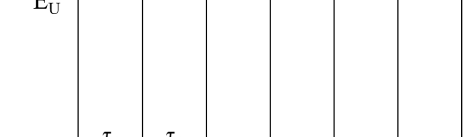
The electrolyte used was a conventional chrome plating bath containing 250 g L-1 CrO3 and 2.5 g L-1 H2SO4 (SCR).The working electrodes were 0.3 cm2 surface area flat copper sheets cut from virgin circuit board plates, and the counter electrode was made of Pb-5%Sb alloy as is usually referred in the literature [2] with anode to cathode areas ratio of 20:1 [5] and the electrolyte volume was 100 ml. CV were done at a sweep rate of 20 mVs-1 at 50 ± 0.1ºC. PD were obtained on the copper cathodes under free convection at 50 ± 0.1ºC during 120 s. Short duration potential steps were applied to the copper cathodes in the plating electrolyte and 1 s current density (CD) transients were analyzed. CE vs. potential curves were recorded for the copper electrodes in the chrome plating bath at 50 ± 0.1ºC considering a simple RC series equivalent circuit. A frequency of 1.5 kHz was chosen for the ac signal because the capacity readings were stable and reproducible in a frequency range from 0.5 to 3 kHz. A potential scan rate of 2 mVs-1 was applied and CE was measured each 25 mV. The SWPO treatments were carried out cycling the electrode potential between an upper potential (EU, during τu seconds) and a lower potential (EL, during τl seconds) at 50 ± 0.1ºC in an open cell under potentiostatic control. A schematic of the SWPO function is shown in figure 1. The shape of the square wave was always symmetric (τu = τl) and the frequency (f) was fixed at 5 Hz (τ = 0.2 s). In all the experiments the time of treatment was 10 minutes (3000 cycles).

Fig. 1: Sketch showing a SWPO signal, alternating between EL and EU at a frequency f = 1/(τl+τu).
CV, PD and SWPO treatments were applied with a potentiostat-galvanostat Princeton Applied Research Mod. 273 with in-built signal generator and controlled by the SoftCorr 2 software. The ac electrochemical technique was applied with a frequency response analyzer Solartron 1255 connected with a potentiostat-galvanostat Solartron 1287 controlled with the Z-plot for Windows v 3.0 software.
In all the experiments a Cu-CuSO4 (sat) reference electrode was used (Eº=0.316 V vs normal hydrogen electrode) and all the electrochemical potentials in this work are expressed in this scale. SEM micrographs were recorded with a Quanta200 FEI equipment (Tungsten filament source). The composition of the coatings was evaluated using EDS. The detector scan mode with a step size of 0.05° and a sampling time of 3 s was used (scan rate 0.0167 º/s). X-ray photoemission spectroscopy (XPS) measurements were performed exciting with a radiation of 1253.6 eV (non-monochromatized X-ray Mg Ka source, 13 kV anode voltage and a power of 300 W). A two-point calibration of the energy scale was performed using sputtered gold and copper samples (Au 4f7/2 binding energy (BE) = 84.00 eV; Cu 2p3/2 BE = 932.67 eV). C 1s at 285 eV was used as charging reference. The hardness of each coating was determined averaging eight readings on its surface with a Shimadzu micro hardness tester with 15g loading during 5s.
3. Results
3.1 Cyclic voltammetry
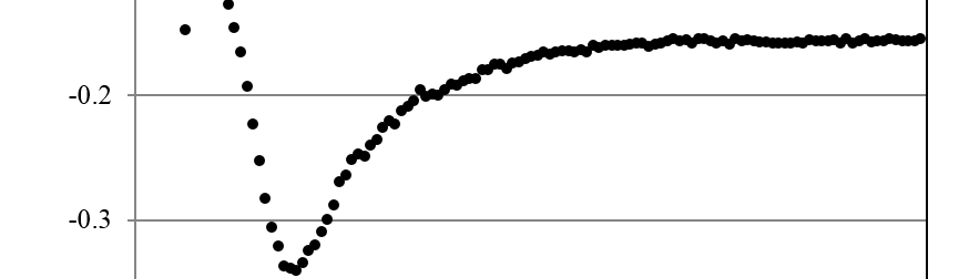
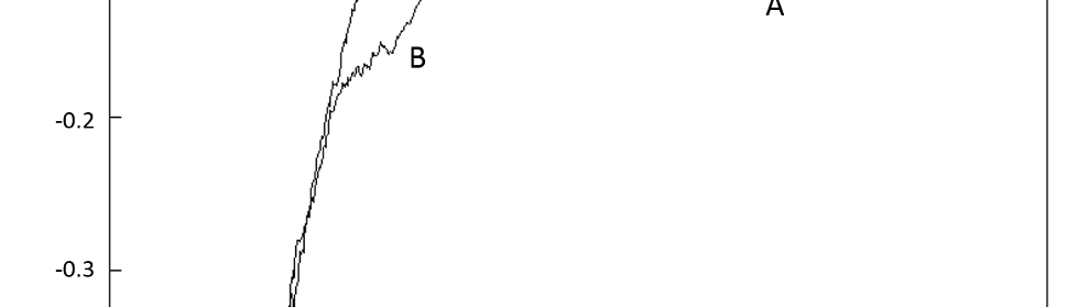
In figure 2 it is shown the first CV cycle of a copper cathode in SCR solution from 0.00 V to -1.20 V. During the forward scan two peaks were detected, marked as A and B. The cathodic processes occurring from -0.20 V to the CD minimum at -0.82 V are usually ascribed [17-21] to the formation of a Cr+3 oxide adsorbed film, formed by the reduction products of the reactions underlying peak A. R. Giovanardi et al [17] proposed an adsorption-desorption mechanism involving chromium species of different oxidation states partially covering the electrode surface:
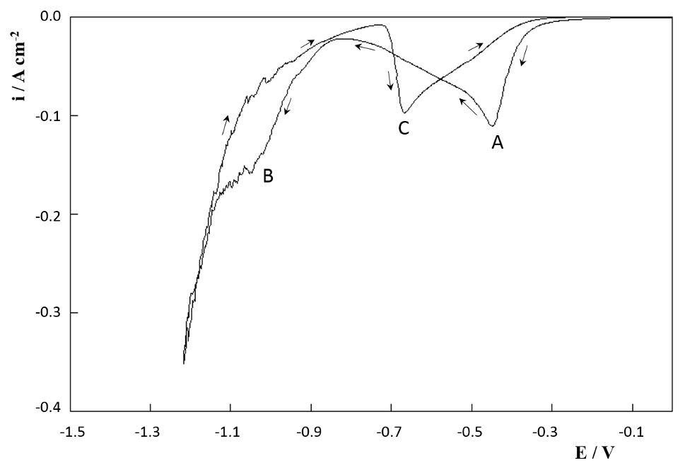
Fig. 2: First CV scan of a copper cathode in SCR electrolyte at 20 mVs-1 and 50º C
Crsol+6 + S + 2 e– → Crads+4 (1)
Crads+4 + e– → Crads+3 (2)
Crads+3 + e– → Crads+2 (3)
Where S stands for copper electrode free surface area with its characteristic surface density of electroactive sites. Crsol+6 is the concentration of Cr+6 in solution and Crads+n represent de chromium species adsorbed on the copper active sites (n=2, 3, 4). When the copper electrode potential is more cathodic than -0.82 V peak B start to grow, related to equation (3) [17] and also to the start of bulk chromium deposition [19, 21]. H2 evolution is negligible on copper cathodes but at sufficiently cathodic potentials it is combined with metallic chromium as unstable hydrides [22]. The decomposition of this hydrides during chrome plating are responsible of the cracking of the coating during electrodeposition [23].
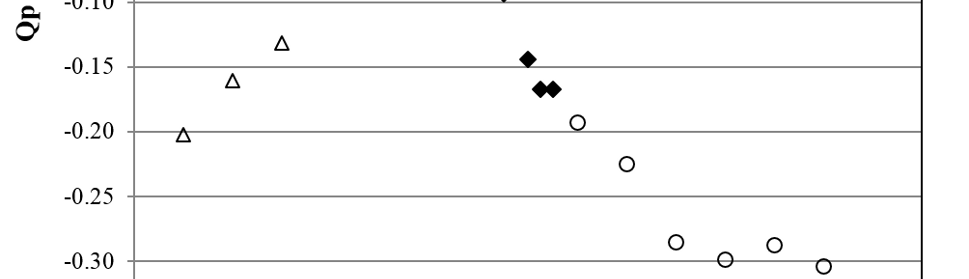
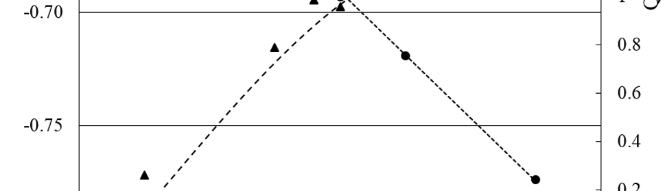
The first backward scan in figure 2 shows one peak (C) at -0.74 V (EC). CD is cathodic for forward and backward scans, indicating that the electrochemical reactions involved are irreversible [17, 24]. EC was measured for switching potentials (SP) between -1.0 V and -1.3 V and the cathodic charge resulting from the integration of the area of peak C (QC) was calculated. As can be seen in figure 3, EC and QC both strongly depend on SP value. The shape of the backward scan on a metallic chromium surface in SCR electrolyte is known to be a flat response [2, 3, 8, 9, 24]. For SP more cathodic than -1.25 V peak C practically disappears (QC ≈ 0) indicating that the entire copper surface is covered with metallic chromium, thus inhibiting equations (1), (2) and (3) due to the absence of free S sites. This behavior indicates that the coverage of the Cu surface with metallic Cr increases with more cathodic SP values. It is important to remark here that for SP more anodic than – 0.80 V peak C does not show up, and this will be addressed again in section 3.3.
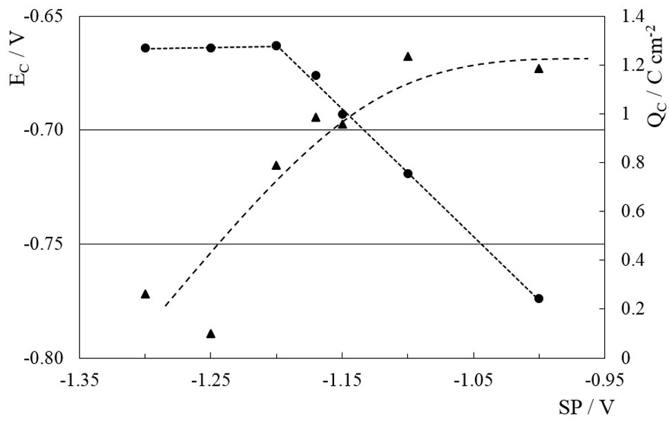
Fig. 3: QC (▲) and EC (●) dependence with switching potential (SP)
Other authors [25, 26] consider that peak A corresponds to Cr+6 to Cr+3 reduction and that its slight shoulder corresponds to incipient H+ reduction, followed by a second passive region before the onset of Cr+6 to Crº reduction and H2 evolution at peak B potentials. L. C. Jiang and D. Pletcher [24, 27] instead, postulated that peak B corresponds to Cr+3 to Crº reduction together with H2 evolution. Survilene found that Cr+2 and hydrogen atoms are involved in the reaction mechanism [28]. There are some discrepancies between different investigators but most of them coincides on the formation of a thin layer very close to the electrode surface, made of Cr+6 reduction products, prior to bulk chromium deposition and that this process is responsible of peak A [29, 30]. The other common issue is that once this layer is formed, there is some evidence of passivation or at least a current reduction between peaks A and B [31, 32].
3.2 Potentiostatic deposits
PD were done on flat copper electrodes in SCR electrolyte at selected potential values corresponding to some of the SP studied in 3.1. In figure 4 a) it is shown the SEM image of the electrode surface for E = -1.10 V. It was confirmed by EDS analysis that isolated chromium crystals of 2 μm average diameter size are obtained over the copper substrate. In figure 4 b) it is shown the SEM image of a deposit obtained at E= -1.20 V were an almost complete layer of chromium deposit is formed. Very small geometric morphologies are observed at higher magnifications (figure 4 c)). The SEM image of figure 5 a) shows the coating obtained at E= -1.25 V, were the minimum of QC is observed (figure 3). In this case the very thin chromium layer is cracked and the entire electrode surface is covered by the metallic chromium deposit and a network of crystals is observed. The SEM pictures of the PDs are consistent with what was inferred from the CV analysis in 3.1. For PDs at more cathodic potentials (-1.25 V > E > -1.35 V) the classic cracked smooth chromium plated surface is obtained (not shown). At higher cathodic overpotentials (E ≤ -1.35 V) globular structures develop, like the “cauliflower” type described elsewhere [33] (figure 5 b)). It is clear from this picture that the cracks of the metallic coating are produced during the buildup of the film because some of the globular structures were grown over previously opened cracks and others are divided by the underlying fissures.

Fig. 4: SEM images of potentiostatic deposits on a copper cathode in SCR electrolyte (50º C during 120 s) at a) -1.10 V, arrows indicate the isolated metallic chromium crystals, b) -1.20 V (5000X). c) zoom of rectangle in b) showing geometric details on the coating (15000X).
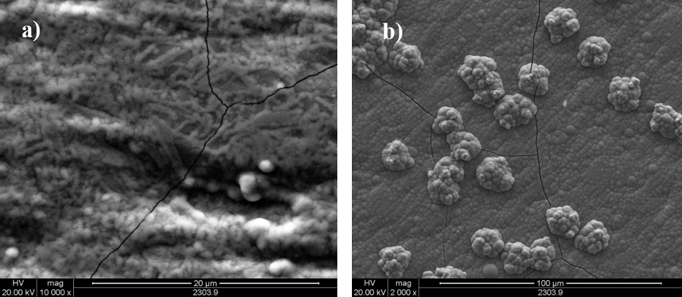
Fig. 5: SEM images of potentiostatic deposits on a copper cathode in SCR electrolyte (50º C during 120 s) at a) -1.25 V (10000X), showing a network of crystals and the first cracks on the coating, b) SEM image representative of metallic chrome deposits for electrode potentials ≤ -1.35 V (2000X).
3.3 Potential steps
Copper cathodes were stabilized during 10 seconds at +0.50 V, then the potential was stepped to Ep and the CD transient was registered during 1 second. Ep was varied from -0.50 V to -1.15 V covering the potential zone between peaks A and B.
CD was integrated for each transient during 1 s and the charge density (Qp) was obtained for each Ep, showing the results in figure 6. For Ep between -0.50 and -0.75 V the transients show diffusion like behavior and the CD transients presented lineal i vs. t -1/2 responses with i≈0 for t=0 (not shown), indicating that a diffusion process is involved and that the following relation holds:
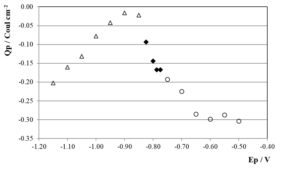
Fig. 6: Qp vs. Ep dependence for potential steps on copper cathodes in SCR electrolyte at 50º C (○ diffusion, ♦ nucleation and growth and Δ flat transient behavior).
i = n F Do1/2 C*/π1/2 t1/2 (4)
were all the variables and constants have their usual meaning. The slope was in average -0.14 ± 0.01. Considering Do ≈ 1×10⁻⁵ cm2s-1 and C* ≈ 1/3 CCrO3 because of polymerization of H2CrO4 [17, 34], we get from equation (4) an estimate of n ≈ 3. This is consistent with Cr+6 to Cr+3 reduction previously described. For Ep between -0.78 and -0.83 V the CD transients show a characteristic nucleation and growth curve (figure 7).

Fig. 7: Characteristic CD transients for Ep= -0.80 V (●) and Ep= -1.00 V (○).
This type of behavior has been assigned by Pletcher et al [24, 27] to the nucleation and growth of holes in a passive layer. This narrow potential range matches quite well with the electrochemical potential of the direct reduction of Cr2O3 to metallic chromium equilibria [35] (Equation (14) in section 4.2). If we consider pH≈-1 and make the temperature correction to 50°C [36] we get, from (15), E50 ≈ -0.82 V. This suggests that the nucleation and growth process could correspond to the reduction of the oxide layer and the birth of new metallic chromium nucleus, living “holes” in the previous passive layer. As was stated in 3.1 the fact that peak C does not appear for SP more anodic than -0.80 V is related with this phenomena. For Ep more cathodic than -0.83 V the CD transients show a flat response characteristic of the PD at short times (figure 7) and Qp is 95% smaller than for Ep ≤ -0,75 V, indicating that a new slow kinetic process starts. As it was shown in the previous section, this corresponds to the growth of the metallic chromium deposit. The direct Cr+6 reduction to bulk metallic chromium starts on the new born chromium phase, through the usually accepted mechanism [24, 25, 27, 31, 34], with the corresponding lower CD at this low cathodic overpotential for this reaction (3.2). When Ep reaches more cathodic values, Cr+6 reduction gets more important and CD and Qp grow again.
3.4 Capacitance vs. potential curves
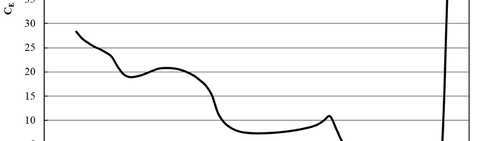
Figure 8 shows the CE vs. potential response for the copper cathodes in the SCR solution at 50 ± 0.1 ºC. There is a very low CE zone between +0.60 V and +0.15 V because of Cu passivation through the formation of an insoluble CuCrO4 film. Near +0.10 V the corresponding Cu active to passive pseudo CE maximum is observed. For E > +0.60 V transpasivity is reached.
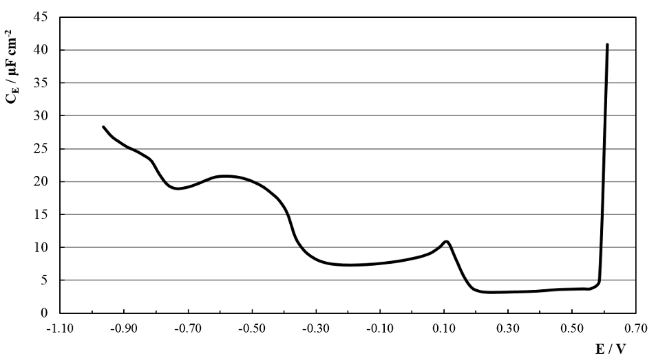
Fig. 8: CE vs. potential curve for a copper cathode in SCR electrolyte at 50º C and 1.5 kHz.
From E = 0 V to -0.30 V a new CE plateau is shown, with a minimum at ≈ -0.20 V indicating that this could be the potential of zero charge (pzc) of the cathode [37].
From -0.30 V to -0.78 V there is a new pseudo CE loop corresponding to the diffusion transients described in 3.3. It is highly probable that this corresponds to the film formation described elsewhere [26, 29, 30_ENREF_26, 34]. Although thermodynamically feasible, the reduction of Cr+6 to Cr+3 is kinetically inhibited until E = -0.30 V generating the pre-plating cathodic film which is widely accepted as high Cr+3 content. For – 0.83 V ≤ E ≤ – 0.78 V after another CE arrest, a different process start, associated to the nucleation and growth depicted in 3.3. For E < – 0.83 V CE continues to grow after a slight shoulder, probably related to equation (3) [17, 28].
3.5 Square wave pulsating overpotential treatment
Based on the preceding results a relatively fast periodic SWPO was applied to the copper cathodes. EL was fixed at -1.30 V, value sufficiently cathodic to obtain the reduced chromium species after peak A and B, but just before diffusion effects become important (3.2 and figure 5). Also from the curves of figure 3, at this EL it is expected to obtain a complete coverage of the copper substrate. The EU values were selected between -0.70 V and +0.50 V to vary the electrode potential through the different capacity plateaus in the anodic direction. Different types of deposits were obtained depending on EU values.
For -0.70 V ≤ EU < -0.40 V the deposits look very similar to the standard bright cracked metallic chromium coatings as in potentiostatic or galvanostatic electrolysis [2, 15]. In the case of setting -0,4 V ≤ EU < -0,2 V the coatings morphology and their metallic luster are almost the same but cracks are absent. It is very interesting to remark that the cracks disappear when EU is more anodic than EA.
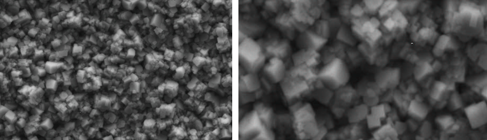
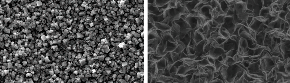
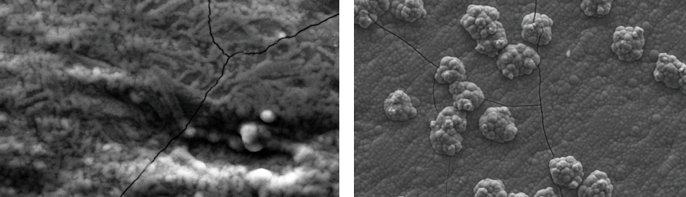
Moving to more anodic EU values, a new type of deposit is obtained, shown in figure 9 a). In these cases the coatings are matt gray and their morphologies are facetted and exhibit a very peculiar structure that is maintained for -0.20 V ≤ EU < +0.30 V, with slight changes in faceting. The average particle size is around 0.5 μm.
When EU reaches +0.40 V and +0.50 V a new coating morphology appears, shown in figure 9 b). This type of coating, matt black, resembles the black coatings prepared with modified electrolytes reported elsewhere [12, 13].

Fig. 9: SEM images of deposits obtained with SWPO treatment on the copper cathodes in SCR electrolyte at a) EU = -0.10 V and b) EU = +0.50 V.
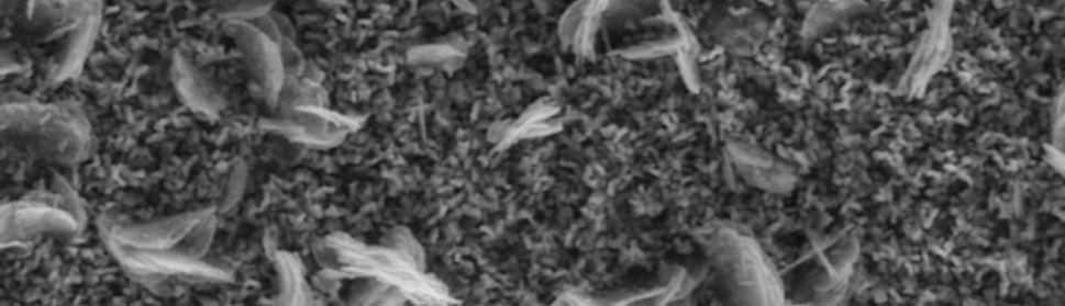
It is very interesting that for EU just in the intermediate zone between the facetted type morphologies and the black coatings, an intermediate mixed coating is obtained (figure 10). In this case it is possible to distinguish both types of structures. This behavior is observed for EU values between +0.30 V and +0.40 V. Finally for EU ≥ +0.60 V no Cr deposit is obtained.
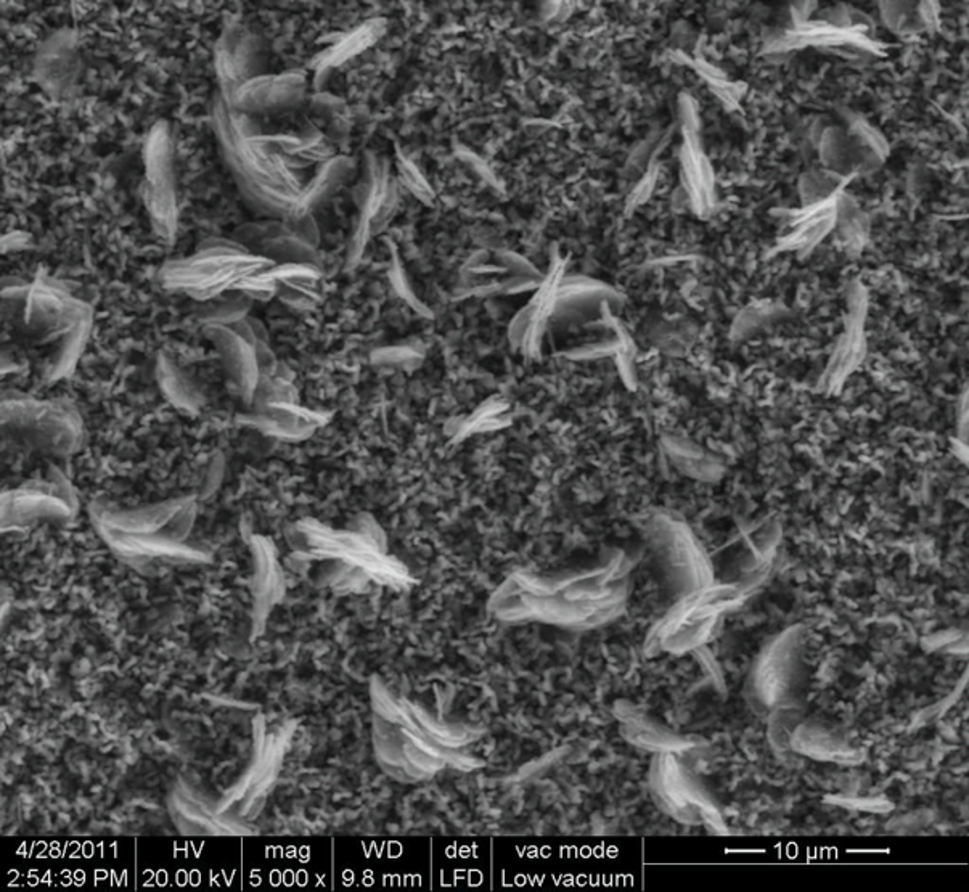
Fig. 10: SEM image of a deposit obtained with SWPO for EU = +0.40 V.
3.6 Characterization of SWPO deposits
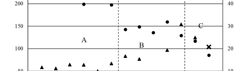
All the coatings obtained with the SWPO treatments were exhaustively washed with double distilled water, fast air dried and micro hardness and EDS quantitative analysis was done. The only elements detected where Cr and O. In figure 11 it is shown the dependence of the oxygen content in weight per cent (O%) with EU. Based on the O% values, it is possible to distinguish three zones: A) -0.70 V < EU ≤ -0.20 V with O% near to 10%; B) -0.20 V < EU < +0.30 V with increasing O% values almost reaching 30% and C) +0.30 V ≤ EU ≤ +0.50 V, a very distinct zone where O% start to grow with a sharp positive slope, reaching 50%. If we make an estimation of the O% for Cr2O3 and for Cr(OH)3 the approximate values are 30% and 50% correspondingly.
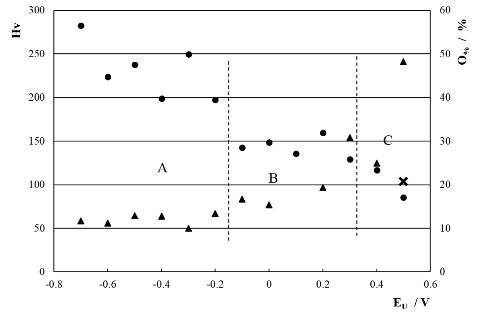
Fig. 11: Surface Vickers micro hardness (Hv; ●) and EDS oxygen content (O%; ▲) of SWPO deposits as a function of EU. ✕ = Hv of substrate. Zones A, B and C are delimited with dashed lines.
In order to correlate the O% behavior with chemical composition of the coating some XPS determinations were done. It was concluded that in zone B the main chromium species were Cr2O3 and in zone C Cr(OH)3. For the particular case of the coating obtained at EU = +0.50 V the composition was 71% Cr(OH)3 and29% CrO3. Accordingly for EU ≥ +0.60 V no deposit was obtained indicating that all the chromium species formed at EL during τl are dissolved at EU during τu.
The surface Vickers micro hardness of the SWPO coatings shown in figure 11 varies with EU from the same value as the substrate at EU = +0.50 V to three times this value at more cathodic EU values. Here again the three different zones arises, A) with an average Hv between 200 and 300, B) with 150 constant value and a pronounced softening for C). The higher Hv values are found for EU more cathodic than -0.20 V, that is when the coating is metallic Cr. The micro hardness was not measured in the cross section of the coatings due to the small thickness of the samples produced in this work (≈ 3 – 4 µm).
4. Discussion
4.1 Current density transients during SWPO treatments
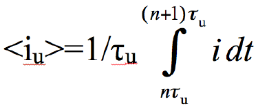
The average CD during application of EU during τu;
 (5)
(5)
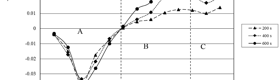
was calculated for n=2000 (200 s), 4000 (400 s) and 6000 (600 s) for each SWPO treatment. The results are shown in figure 12. The dependence of <iu> with EU shows that for EU more cathodic than -0.20V the CD is always cathodic and that <iu> practically does not vary with time. This last behavior is probably related with the very smooth surface of the deposits obtained for these samples.
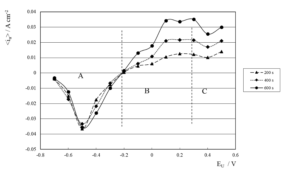
Fig. 12: Average CD for 200, 400 and 600 s of SWPO treatment as a function of EU. Zones A, B and C are delimited with dashed lines.
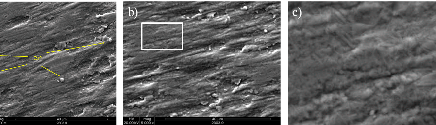
For EU more anodic than -0.20 V, <iu> > 0, indicating that anodic processes prevails on the electrode during τu. It is also evident that <iu> increases with time due to the surface roughening of the deposits during treatment (figures 9 and 10). Finally for EU = -0.20 V, <iu> = 0, indicating that no net faradaic process occurs during τu and that it is invariant with time of treatment. The SEM images of figure 13 shows the morphology of this coating where it is possible to see a cubic structure with very well faceted crystals. It is interesting to remark that this point coincides with the possible pzc of the system as seen on CE vs. E curve (figure 8). This EU value is a transition point from which to more cathodic values the deposits are metallic chromium and to more anodic values the coatings are facetted structures with high oxygen content. As was observed on data of figure 11 we can differentiate zone A, B and C on <iu> vs. EU dependence on figure 12.
Fig. 13: SEM image of deposit obtained with SWPO treatment. EU =-0.20 V. a) 10000X; b) 25000X.
When we analyze the complementary average CD during the cathodic hemicycle of the SWPO treatment, <il>, with integration limits in (5) from (n+1) τl to (n+2) τl for n = 2000, 4000 and 6000 at EL = -1.30 V, we find that (<il>/<iu>)ti ≈ 10. This is consistent with the asymmetric efficiencies of the deposition and dissolution processes in chrome plating [2, 5, 38]. Based on this, we can consider that practically all the reduced chromium species obtained at EL during each τl, are electrochemically modified during next τu depending on EU value. W. R. Rosas and A. Robin showed that for very short times the thin layer necessary to obtain metallic Cr during chrome plating is not formed [31_ENREF_27], so during the SWPO treatment the formation of this type of deposit will depend on EU. In that way, for EU values more cathodic than -0.20 V (cathodic <iu>) it is possible to keep intact or even to build up the film during τu. As previously depicted in 3.5 the deposits obtained in this range of EU values are all metallic chromium, with the lowest oxygen content. The fact that for EU between -0.40 and -0.20 V the deposits are crack free is associated with the elimination of chromium hydride as in pulse reverse chrome plating [23].
For EU values more anodic than -0.20 V the morphology and composition of deposits change abruptly and facetted crystallites are clearly seen. It is also verified that for gradually more anodic EU values the chromium oxides composition moves from Cr2O3 towards Cr(OH)3.nH2O. This was confirmed by EDS and XPS measurements. This evidence is also consistent with the oxygen content and the softening of the coatings (figure 11).
4.2 Thermodynamic considerations
From a thermodynamic point of view, the possible processes that can occur on the electrode during SWPO treatment, depending on the electrochemical potential and based on the chemical species found after the SWPO treatment are:
Cr+3 + 4H2O = HCrO4– + 7H+ + 3e–
E0= 1.034 + 0.138 pH + 0.0197 log(HCrO4–/Cr+3) (6)
Cr(OH)3.nH2O + H2O = HCrO4– + 4H+ + 3e–
E0= 0.801 – 0.0788 pH + 0.0197 log(HCrO4–) (7)
2Cr(OH)3.nH2O + H2O = Cr2O7-2 + 8H+ + nH2O + 6e–
E0= 0.785 – 0.0788 pH + 0.0098 log(Cr2O7-2) (8)
Cr+2 + 4H2O = HCrO4– + 7H+ + 4e–
E0= 0.311 + 0.1379 pH + 0.0147 log(HCrO4–/Cr+2) (9)
Cr+2 + (3+n)H2O = Cr(OH)3.nH2O + 3H+ + e–
E0= -0.027 – 0.1773 pH – 0.0591 log(Cr+2) (10)
2 Cr+2 + 3H2O = Cr2O3 + 6H+ + 2e–
E0= -0.228 – 0.1773 pH – 0.0591 log(Cr+2) (11)
Cr + (3+n)H2O = Cr(OH)3.nH2O + 3H+ + 3e–
E0= -0.676 – 0.0591 pH (12)
Cr+2 = Cr+3 + e–
E0= -0.723 + 0.0591 log(Cr+3/ Cr+2) (13)
2Cr + 3H2O = Cr2O3 + 6H+ + 6e–
E0= -0.895 – 0.0591 pH (14)
Cr = Cr+3 + 3e–
E0= -1.060 + 0.0197 log(Cr+3) (15)
Cr = Cr+2 + 2e–
E0= -1.229 + 0.0295 log(Cr+2) (16)
Based on the results obtained in 3.1 it is evident that some of these reactions are strongly inhibited on the Cu electrode (e.g. 6-8). During the cathodic hemicycle of the SWPO, species like Cr+3, Cr+2 and Crº will be formed on the electrode surface. The possible mechanisms could be quite complex and will be the result of a mix of some of the processes listed above. But considering the experimental evidence that for EU more anodic than +0.60 V all these intermediate species are dissolved, suggests that Cr+2 could play a role on the processes occurring at EL. This assertion can be postulated because the only equation that thermodynamically allows the direct oxidation of chromium species to a soluble compound at this potential value is (9), after correcting the right potential value at 50º C. If we assume that the main active chromium species generated during τl is Cr+2 we can also understand through equations (10) and (11) how the deposits depicted in 3.5 for EU between -0.20 and +0.30 V could be grown. The continuous build up of the gray and black chromium oxides/hydroxides films described in 4.1 suggests that the Cr2O3 and Cr(OH)3.nH2O are irreversibly formed on the cathode surface. That means that during each cycle of the SWPO signal Cr+2 is formed at EL during τl,and then this Cr+2 is oxidized at EU during next τu to the corresponding Cr+3 compound. As this is a dynamic model, not in equilibrium, the thermodynamic considerations has to be considered as feasibility limits.
For the metallic chromium deposits obtained for -0.70 V ≤ EU < -0.20 V it is clear that during τu at this electrode potentials the pre plating layer necessary for obtaining metallic chromium is not destroyed. In that way the usually accepted chrome plating mechanism will be possible during both hemicycles of the SWPO treatment (τl + τu).
5. Conclusions
Based on preliminary cyclic voltammetry, potentiostatic deposits, potential steps and CE vs. potential curves, it was designed a square wave pulsating overpotential treatment that allows the obtaining of coatings of different chrome species on copper substrate starting from a standard chrome plating bath. Properly adjusting the frequency and lower and upper potential values of the SWPO signal it was possible to obtain cracked and crack free metallic chromium coatings and chromium oxide and hydroxide mixtures films. The oxygen content and surface hardness of these coatings can be controlled as well. Different deposit morphologies were obtained: smooth metallic surfaces, very well facetted crystallites arrangements and leaf type structures. The color of each type of coating also varied from white bright metallic finish for the cracked and crack free metallic coatings, light gray for the facetted crystallites, dark gray for the mixed type coating and matt black for the high hydroxide content leaf type structure. This last type of coating was found to be very similar to the black deposits used for solar energy absorption panels.
Some thermodynamic considerations were made regarding the possible mechanism of coating build up during the SWPO treatment and some insight in deposition mechanism could be done.
6. Acknowledgements
The author thank to the Comisión de Investigaciones Científicas de la Provincia de Buenos Aires (CICPBA) for the financial support to carry out the present research paper.
- Lausmann, G.A., Surf. Coat. Technol. 1996(86-87): p. 814-820.
- Mandich, N.V. and Snyder D.L., Modern Electroplating Fifth Edition, p. 205-248. Schlesinger M. and Paunovic M., Editors, J. Wiley & Sons. (2010).
- Newby, K.R., ASM Handbook, Vol. 5, Surface Engineering. 1994, ASM International, p. 177-191
- Sargent, G.J., Trans. Am. Electrochem. Soc., 1920. 37.
- Wolf G., E. Halwax and Kronberger H., Met. Finish., 2010. 108(1): p. 19-27.
- Protsenko V. and Danilov F., Electrochim. Acta, 2009. 54: p. 5666-5672.
- Zeng, Z., Wang L., Liang A. and Zhang J., Electrochim. Acta, 2006. 52: p. 1366-1373.
- Howarth, J.N. and Pletcher D., J. Appl. Electrochem., 1988. 18: p. 644-652.
- Mooney, T., Corrosion: Fundamentals, Testing, and Protection, p. 772–785. ASM International (2003).
- Aguilar, M., Barrera E., Palomar-Pardavé M., Huerta L. and Muhl S., J. Non-Cryst. Solids, 2003. 329: p. 31-38.
- G. B. Smith, R. C. McPhedran and Derrick G. H., Appl. Phys., A36, 193-204 (1985).
- Popov, B.N., White R. E., Slavkov D. and Koneska Z,J. Electrochem. Soc., 1992. 139(1): p. 91-98.
- Aguilar-Sanchez, M., Palomar-Pardavé M., Romero-Romo M., Ramírez-Silva M. T., Barrera E. and Scharifker B. R., J. Electroanal. Chem. 2010. 647: p. 128-132.
- Pesco, A.M. and Cheh H.Y., Modern Aspects of electrochemistry, p. 251-293. Plenum Press (1989).
- Puippe, J.C. and Leaman F., Theory and practice of pulse plating. American Electroplaters and Surface Finishers Society, Publisher (1986), p. 109-117.
- Chandrasekar, M.S. and Pushpavanam M., Electrochim. Acta, 2008. 53: p. 3313–3322.
- Giovanardi, R., Soragni E., Fontanesi C. De Renzi V., Del Pennino U. and Foresti M. L., J. Electroanal. Chem., 2005. 576: p. 243-252.
- Baraldi, P., Barani G., Fontanesi C. and Soragni E., Intermetallics, 2000. 8: p. 313-319.
- Soragni, E., Fontanesi C., Barani G. and Ganzerli V., J. Appl. Electrochem., 2000. 30: p. 1069-1079.
- Vashchenko S. V., Solodkova L. N. and Solov’eva Z. A., Russ. J. Electrochem.; Vol. 36, No. 9, 2000, pp. 947-951.
- Baraldi, P., Soragni E., Fontanesi C. and Ganzerli V., J. Alloys Compd. 2001. 317-318 p. 612-618.
- Gabe D. R., J. Appl. Electrochem., 1997. 27: p. 908-915.
- Saghi Beyragh M.R., Khameneh Asl Sh. and Norouzi S., Surface & Coatings Technology 205 (2010) 2605–2610
- Pletcher D. and Lin-Cai J., J. Appl. Electrochem., 1983. 13: p. 235-243.
- Dobson S.J. and McCormick M., J. Appl. Electrochem., 1987. 17: p. 303-314.
- Saiddington, J.C. and Hoey G.R.,J. Electrochem. Soc., 1970. 117(8): p. 1011-1020.
- Jiang, L.C. and Pletcher D., J. Appl. Electrochem., 1983. 13: p. 245-252.
- Survilene S., Russ. J. Electrochem. Vol. 34, No. 5, 1998, pp. 506-512.
- Ryan, N.E., Met. Finish., 1965(January): p. 46-50.
- Ryan, N.E., Met. Finish., 1965(February): p. 73-74.
- Rosas, W.R. and Robin A., J. Appl. Electrochem., 2001. 31: p. 531-536.
- Fang, J.L., N.J. Wu, and Wang Z.W., J. Appl. Electrochem., 1993. 23: p. 495-499.
- Leisner, P., Bech-Nielsen G. and Moller P., J. Appl. Electrochem., 1993. 23: p. 1232-1236.
- Hoare, J.P.,J. Electrochem. Soc., 1979. 126.
- Pourbaix, M., Atlas of Electrochemical Equilibria (1974).
- Bratsch, S.G., J. Phys. Chem. Ref. Data, 1989. 18(1).
- Conway, B.E., Theory and Principles of Electrode Processes, New York: The Ronald Press Co. (1965).
- Griffin, J.L., Plating, 1966(February): p. 196-203.
PDF Version of the article |
Flash Version of the article |
|
| [qr-code size=”2″] | ||