
The principles of energy dispersive x-ray fluorescence (EDXRF) technique and its elemental analysis applications were described in some books and reviews [1-4]. PCBs are an important application for nickel-phosphorus (NiP) coatings, on top of which, additional gold and/or palladium coatings are applied. Phosphorous concentration of chemically (or electroless) deposited nickel-phosphorus (NiP) coating can be analyzed in nondestructive manner in atmosphere without stripping Au and Pd coatings. The FP-based WinFTM software allows a reliable determination of both the mass per unit area of the NiP layer and its P concentration [5]. The reproducibility and accuracy of the analysis is verified by means of certified standard reference material. Their quantification is traceable to accurate mass per unit area primary standards analyzed by several suitable techniques [6]. The typical measurement spot size is about 1mm, but in case of micro-spot instruments even smaller spot sizes (less than 100 µm) are achievable.
1. Measurement protocol
The Figs. 1–3 depict a typical PCB analysis. A certain number of pre-defined and programmed pads (positions) are measured automatically.
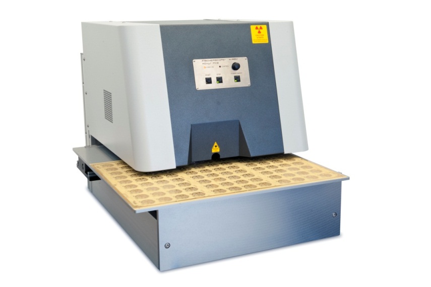
Fig. 1: The Fischerscope© XDV-µ-PCB is designed for PCB testing. Automatic testing even on large boards can be performed by means of the motorized stage. The video image controlled pattern recognition software ensures a correct measurement at the predefined positions.
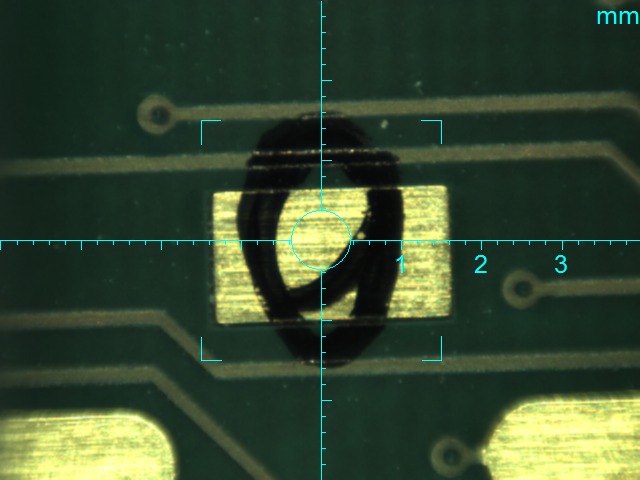
Fig. 2: A Fischerscope© XDV-SDD measures this pad for the Au top layer and NiP layer beneath. The measuring spot size is defined by an aperture of Ø 0.6 mm. The comparably large spot is desired to obtain spectral intensity of about 30,000 cps.
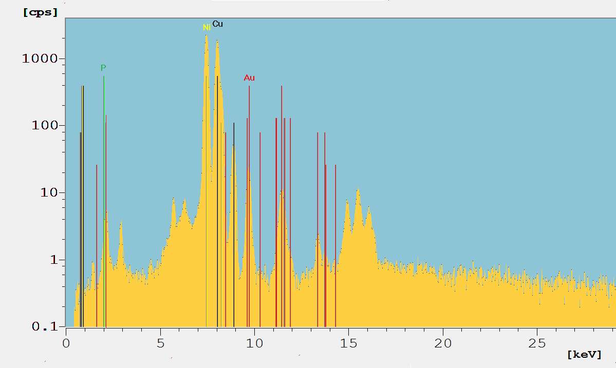
Fig. 3: The spectrum from the PCB sample in Fig.2. The characteristic fluorescence lines are labeled by the respective element symbol. Spectrum in log scale.
2. EDXRF measurement of NiP layers
A common non-direct method [7] requires a substrate of iron and this method has been used previously for many years. It uses the fluorescence intensities of the Ni-layer (Ni-K lines) and of the Fe substrate (Fe-K lines). On other substrates, as in the example presented here – Cu, direct measurement of NiP thickness requires the effective excitation and the reliable detection of the characteristic P-K-radiation, directly. With the Fischer Technology equipment described in this paper NiP layers can be measured on any substrates even when NiP layers are very thin. Of course, the considerably small information depth has to be taken into account as described in more detail in [5,8,9].
Other considerations for the direct EDXRF measurement of PCB NiP layers include:
- The P-K-signal is small compared with the fluorescence signals of Ni or Cu.
- The NiP layer is normally coated with Au and in some cases also with Pd. NiP is not the top layer in any case.
- The Pd layer above may contain P up to 4 wt-%.
Optimal P-K-excitation
The measurement can be performed with “standard conditions” (operation voltage = 50 kV and 10 µm Ni primary filter) – optimal for Au, Ni and Pd excitation. However, a reduction of the X-Ray tube voltage improves the signal vs. background ratio for the P-K-peak. But the improvement of P determination is accompanied with a poor excitation of the higher energy emissions of Ni and Au. As noted above, the higher tube voltage is needed. The solution is combining the two excitation modes within one measurement. The multiple excitation approach for routine NiP analysis is described in reference [5,8,9].
Single excitation can be effectively used with polycapillary X-Ray lenses [10]. The spectrum shown in Figure 4 demonstrates this. It has a sufficient low background for the P-K-peak and effective excitation of Ni-K. This is a result of the energy band pass effect of the polycapillary.
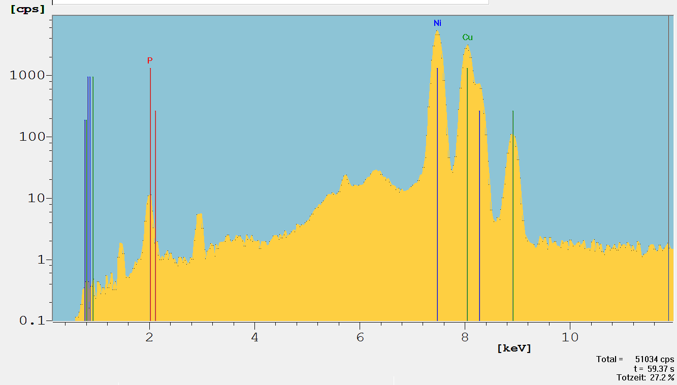
Fig. 4: Spectrum of a 5.2 µm NiP12/Cu/PCB sample measured with a Fischerscope XDV-µ equipped with a polycapillary X-ray lens (50 kV, Mo tube, no filter). Spectrum in log scale.
The traditional primary beam collimation by an aperture (in the example of Figs. 2 and 3 the size of the aperture is Ø 0.6 mm) yields roughly the same spectral intensity as the polycapillary lens of Figure 4. The measurement uncertainty due to counting statistics can therefore be expected to be similar. However, the first system needs two excitation modes ( two measurements) instead of a single one for the polycapillary. The striking difference, however, is the measuring spot size which is less than 50 µm diameter for the system with the polycapillary lens and approximately 1 mm diameter for the aperture system. For samples with large test pads (cf. Fig. 2) the large spot size works well, IPC standard 4556, for example requires measurement on a 1.5 x 1.5 mm pad. In contrast to it, a wide variety of applications ask for small measuring spot sizes and the polycapillary lens system is the only choice.
The effect of Au and Pd top layers
The following considerations are true both for traditional aperture systems (e.g. the XDV© – SDD, Fig. 2) and polycapillary instruments (e.g. Fig. 1). The determination of the (thin) Au and Pd layers is an intrinsic application of PCB testing [11,12]. Regarding the possibility of NiP analysis beneath them represents an important extension of EDXRF capability. Obviously, these top layers impact the NiP testing due to absorption and peak overlap. Au and Pd reduce the already low intensity of P-K by absorption. Au-M-radiation completely overlaps with P-K, too. The following Figures 5 and 6 illustrate these effects:
a) Pd
The P-K-peak (energy about 2 keV) of a 5 µm thick NiP10 layer is shown in Figure 5 (blue spectrum).
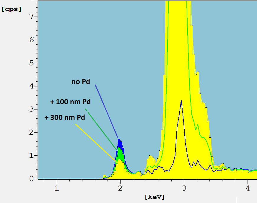
Fig. 5: Detail of spectra of the NiP layer coated with Pd layers of different thickness. XDV-SDD,W-anode tube, 50 kV, 10 µm Ni primary filter. See text.
In addition, the respective spectra top layers of 100 nm (green) and 300 nm Pd (yellow) are shown. The Pd-L-peaks at about 3 keV increase with Pd thickness. The blue peak for no Pd at 3 keV is from Ar-K radiation from the air path above the sample, being excited by the primary beam. The corresponding intensity of the P-K-peak decreases with increasing Pd. This is simply due to absorption and the WinFTM© software does take it into account when calculating the P content.
Another effect that will restrict the P determination in the NiP layer in practice is the P content of the Pd layer. The evaluation software cannot distinguish between P in Pd and P in Ni. The composition of NiP can only be analyzed if the Pd composition is known. In this case the Pd-P-composition has to be defined prior to the analysis (cf. DefMA setup [13]).The order of magnitude of this influence can be estimated. The P concentration of 4 wt.% of a 100 nm thick Pd layer causes a P shift in a 3 µm thick NiP layer of -1 wt. % P. Therefore, the uncertainty of the P-concentration of the Pd layer should be low, on the order of less than 1 wt. %.
b) Au
Starting with the same NiP spectrum as in Figure 5, the blue spectrum in Figure 6 shows a well separated P-K-peak (energy about 2 keV) of a 5 µm thick NiP10 layer. When plated with gold the Au-M emissions of a 50 nm (green) and 100 nm (yellow) layer do overlap with P-K completely. The P-K-peak is not separated and only the sophisticated WinFTM© peak de-convolution software can resolve the P-K lines and accurately calculate P concentration. The experimental findings discussed below show that Au layers of more than 100 nm prevent a reliable measurement of the P concentration of NiP.
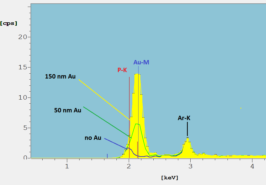
Fig. 6: Detail of spectra of a NiP layer coated with Au layers of different thickness. XDV-SDD, W-anode tube, 50 kV, 10 µm Ni primary filter. See text.

Fig. 7: Detail of the spectra of a sample NiP12/Cu/PCB (same as Fig.4, blue) and a sample of 50 nm Au/96 nm Pd/ 3.2 µm NiP9.3/ Cu/PCB (yellow). XDV-µ-PCB, polycapillary X-ray optics, Mo-anode tube, 50 kV, no primary filter. Spectrum in log scale.
Figure 7 shows the spectrum of a sample with both Au and Pd top layers. The thickness of both layers, 50 nm Au and 96 nm Pd) are measured simultaneously together with the NiP thickness and composition. Table 1 presents the results.
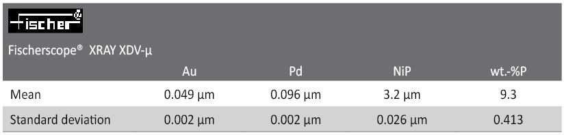
Tab. 1: Test report. Evaluation of five readings (repeatability conditions) of the sample in Fig. 7. XDV-µ-PCB, polycapillary X-ray optic, Mo-anode tube, 50 kV, no primary filter.The measuring time was 60 s.
The standard deviation for the P-concentration is excellent (0.4wt.% for 60 s measuring time, cf. Table 1. It should be noted that a high total spectral intensity of more than 50,000 cps is the result of very high flux excitation by the polycapillary emitted from a relatively small measuring spot of less than 50 µmØ. In the case of a standard aperture beam collimation the total measuring time for similar precision is expected to be a factor of 2-3 longer to achieve the same total counting statistics.
The absorption correction for the Au and Pd top layer works quite well in the WinFTM© software. Nevertheless, certain physical and technical conditions can void a reliable measurement of buried NiP layers. Strong attenuation (which cannot be corrected very accurately) becomes evident for thick top layers. This is observed for Pd >400 nm and/or Au >70 nm as a rule of thumb. The precision of the measurement is affected by the thickness of the Au and/or Pd layers, of course.
3. Certified standard reference material for calibration
As shown in the previous section, the thickness and the composition of electroless deposited NiP layers can be measured by XRF in air with very good precision. Certified reference material is essential for traceable analysis. In general the base material and the layer stack of the reference material or standards should be similar to the measured samples. In addition, NiP standards with Au and Pd surface coatings must be included in a set of standards covering the required measuring range. Nonetheless the real analytical challenge resides in reliable quantification of the NiP layers.
This section deals with the challenges of producing reliable NiP reference material which include,
- the manufacturing of NiP foils and NiP coated standards,
- the subsequent test of NiP material for homogeneity (uniformity),
- the quantification of the mass per unit areas of P and Ni by gravimetric analysis, by standard-less FP (fundamental parameters) based XRF and by destructive chemical analysis,
- the production and characterization of Au and Pd coated NiP material on PCBs.

Fig. 8: Different regions for the XRF information. The primary beam (red) irradiates only a small part of the layer. The information depth for P is < 1 µm but for Ni it is about 20 µm, which is dictated by the escape depth of the analyte energies.
The homogeneity of standard reference material (SRM) is an imperative prerequisite for its use in calibration of XRF analysis. This demand results mainly from the small information depth of the P-concentration combined with the small dimension of the measuring spot size, cf. Figure 8. The typical information depth of a specific fluoresced radiation is given mainly by the absorption properties of the sample matrix on the fluoresced emission. Strong absorption means small information depth. The P-concentration is calculated mainly from the P-K-fluorescence intensity. The information depth can be defined as the reciprocal linear attenuation coefficient of the relevant radiation [5]. A value of less than 1 µm is found for the energy of P-K (about 2 keV) in the predominantly Ni matrix.
Optical Emission Spectrometry with ICP excitation sources (ICP-OES) is used for an independent determination of the masses of Ni and P of a given piece of material (see below). The respective results are valid for the total dissolved NiP layer of the specimen. It can be compared with the XRF readings only if a certain uniformity of the layer is obtained.
The homogeneity of the NiP material has been checked by the following tests:
- An XRF element concentration map of the full area (typically a few cm2) in order to detect possible lateral non-uniformity. Normally 100 – 200 different positions have been analyzed for each specimen in order to obtain a good average value for each specimen.
- NiP foils have been measured (mapped) from both sides.
- Coulometric etching of the foil to obtain spots at different depth for analysis to obtain a ho-mogeneous P concentration with respect to depth (cf. [5], Fig. 9).
- GD-OES (Glow Discharge – Optical Emission Spectrometry) for depth profiles and electron microprobe analyses for surface near composition.
Measurement of NiP material from different sources by different laboratories has been found to be uniform within + 0.3 wt.% P. This value represents also a lower limit for the uncertainty of the SRM.
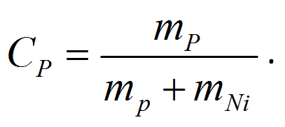
The traceability of the NiP data of the SRM is obtained by the mass determination of P and Ni (mP and mNi) of a piece of NiP with a well-defined area A. This can be performed by a calibrated ICP-OES measurement. The mentioned homogeneity guaranties that the P concentration (CP) which is defined as the mass ratio
(1)
is also valid for the near surface region that corresponds to the information depth. It means we can compare XRF with ICP-OES data and use the chemical analysis for traceability.
The specimens used for SRM have been carefully analyzed by standard-less XRF (WinFTM© software). Coated base materials (Al, Fe, and Cu-PCB-substrate) and self-supporting NiP foils have been investigated. Randomly selected samples have been analyzed by ICP-OES in different labs. The respective results have been used to calibrate the standard-less XRF readings (Fig. 9). The scattering with respect to the regression function is caused probably by non-uniformities (non-homogeneities) of the foil material and by ICP sample prep (dissolution and dilution) effects.
![Fig. 9: The standard-less XRF results for the P concentration correlate well with the ICP-OES results. From [6].](https://www.jept.de/wp-content/uploads/2014/02/pic9.png)
Fig. 9: The standard-less XRF results for the P concentration correlate well with the ICP-OES results. From [6].
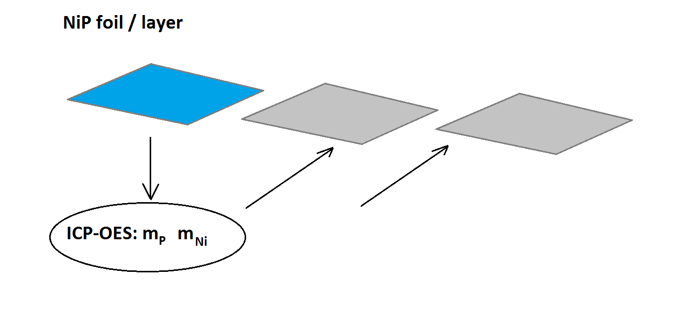
Fig. 10: ICP-OES results from several aliquot samples of the primary foil and standard-less XRF of the foil are applied to “sister foil pieces”– see the text below.
Primary NiP standards
13 different NiP foils have been analyzed, cf. Table 2. 3-6 aliquots of each foil have been analyzed by ICP-OES for their absolute masses of Ni and P (mP and mNi) given in element-wt% and mg). In addition the area and the weight of the foils have been measured. Aliquots of the same foil (typically two pieces) were sent to three ISO-certified analytical laboratories (details cf. [6]). The deviations between the masses per unit area results of the different labs and our gravimetrical data were on the order of 2-5% relative. The same is true for the calculated P concentration, according to Eq. (1). Finally, these data have been used to certify the remaining “sister pieces” of each sample (Fig. 10). Typically two specimens from each NiP foil batch are retained and now represent primary standards. Table 2 lists these NiP foil primary standards.
In the same manner NiP coated PCB material has been characterized by ICP-OES. The sample sheets have been carefully prepared for ICP-OES analysis. Well-defined areas were cut from the coated boards. The mass per unit area and the composition of the NiP coatings have been measured by XRF and ICP-OES in the same way as for the foils described above. The only difference was the lack of gravimetric testing. At the end a number of primary standards with traceable NiP thickness and composition data (Tab. 3) have been generated.
NiP thickness
As described, raw XRF measurement is in terms of mass per unit area. To obtain the thickness, mass per unit area is divided by the density (g/cm3). This requires calculating NiP density as a function of the P concentration. The WinFTM software [13] uses the following density representation for multiple component layers (alloys):

(2)
where ρj is the density of the component j with the concentration Cj. The value of the P density ρP = 4.5 g/cm3 is derived from an empirical graphical representation ρP = f(CP) published in reference [14].
The thickness values listed in the Tables 2-4 are derived from the masses per unit area using this derivation. Other densities are possible, because ρP may vary with plating process.
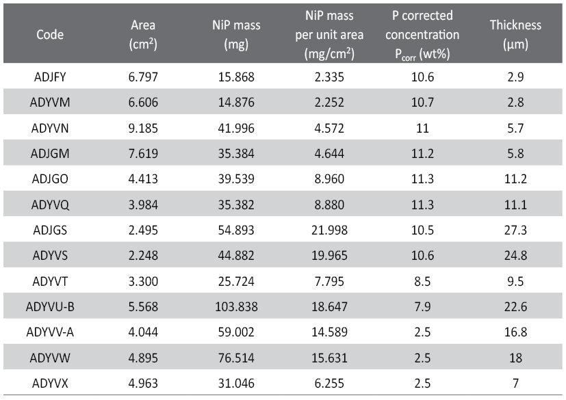
Tab. 2: Primary NiP foil standards. The total mass NiP is derived from ICP-OES, weighing the foils and determining the area of each foil sample with optical methods. The NiP masses per unit area and the P concentrations of the primary standards are XRF results that are obtained from corrected (calibrated) measurements using the ICP-analyzed (and destroyed) sister sample results for XRF calibration. The thickness values are derived from the primary mass per unit area and P-concentration data to calculate NiP densities. The typical standard uncertainty for the amount of P is on the order of 0.3 wt%.

Tab. 3: Primary NiP/PCB standards forPCB application. The total mass NiP is taken from ICP-OES. The areas of the samples have been measured with optical methods. The NiP masses per unit area and the P concentrations are XRF results that are corrected (calibrated) using the data from the ICP-analyzed (and destroyed) sister samples (see Tab. 2). The thickness values are derived from the primary mass per unit area and P-concentration data to calculate NiP densities.
Au and Pd top layers
SRM with sputtered Au and Pd top layers are made from NiP/Cu(PCB) material that has been characterized before the sputter deposition of the surface coatings [15]. The XRF values for Au and Ni masses per unit area (thickness) are determined and certified with thin Au and Pd SRM’s as described in references [16,17]. The forthcoming standards (Tab.4) are tailor made for the calibration of P-determination beneath thin Au and/or Pd layers. They should be applied in combination with Au/Pd/Ni-standard calibration foils (metallic Ni, 0% P) over uncoated PCB material [18].
![Tab. 4: Additional reference standards of Au/Pd/NiP/Cu(PCB) [12]. The thickness of the NiP layer is about 4.5 µm an the P concentration is about 10 wt.%.](https://www.jept.de/wp-content/uploads/2014/02/tab4.jpg)
Tab. 4: Additional reference standards of Au/Pd/NiP/Cu(PCB) [12]. The thickness of the NiP layer is about 4.5 µm an the P concentration is about 10 wt.%.
4. Conclusions
Phosphorus analyses of NiP can be done using various methods, being destructive and non-destructive. The advantage of XRF technique is its non-destructive nature and the ease of use due to the lack of sample preparation. A strong argument in favour of EDXRF analyses is the fact that thickness and composition can be obtained in one step. The final conclusions are summarized in Table 5.
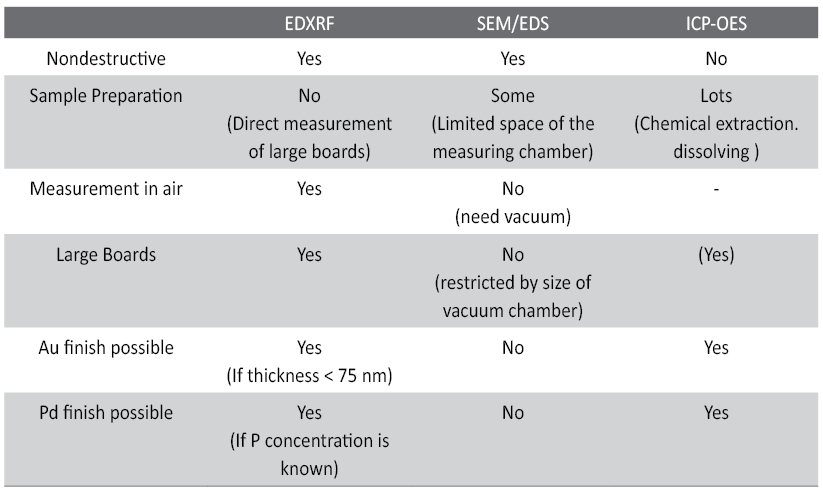
Tab. 5: Qualitative comparison between different analytical techniques for the determination of phosphorus content in electroless Ni-coatings.
References
- B. Dziunikowski (Ed.), “Energy Dispersive X-Ray Fluorescence Analysis”, Elsevier, 1989.
- B. Beckhoff, B. Kanngießer, N. Langhoff, R.Wedell and H.Wolff (Eds.), “Handbook of Practical X-Ray Fluorescence Analysis”, Springer, 2006.
- P.J. Potts and M. West (Eds.), “Portable X-Ray Fluorescence Spectrometry: Capabilities for in situ Analysis”, The Royal Society of Chemistry, Cambridge, 2008.
- M.S. Shackley (Ed.), “X-Ray Fluorescence Spectrometry (XRF) in Geoarchaeology”, Springer, 2011.
- V. Rößiger and W. Klöck, „Messung des Phosphor-gehaltes von Chemisch-Nickel-Schichten mit Röntgenfluoreszenz”, in „Galvanotechnik“, Leuze Verlag, 2012, p. 1-8.
- Fischer Traceability Report WK 2013 01.
- V. Rößiger and G. Conrad, Metalloberfläche München, 43 (12), 1989, p. 569.
- M.Haller, J. Bogert, R. Boyle, V. Rößiger and W. Klöck, “Direct Determination of Phosphorus Content in Electroless Nickel Plating Using X-ray Fluorescence (XRF) Spectroscopy”, IPC APEX EXPO Conference Proceedings, 2013.
- M.Haller, J. Bogert, R. Boyle, V. Rößiger and W. Klöck, “Determining Phosphorus Content in EN Plating Using XRF Spectroscopy”, The PCB Magazine, January 2014, p. 38.
- V. Arkadiev and A. Bjeoumikhov, in “Handbook of practical X-Ray fluorescence analysis”, Springer 2006, p. 89.
- Fischer application note vr0615 “Analysis of small structures using the XDV-µ-SDC”, 2006.
- S. Dill and V. Rößiger, “Coating thickness measurement of thin gold and palladium coatings on printed circuit boards using X-ray fluorescence”, Circuit World, 37 (2), 2011, p. 20.
- V. Rößiger and B. Nensel, in “Handbook of practical X-Ray fluorescence analysis”, Springer 2006, p. 554.
- ASTM Special Technical Publication No. 265, “Electroless Nickel Plating”, 1959.
- Fischer Traceability Report WK 2014 02, in prep.
- Fischer Traceability Report SD 2012 02.
- Fischer Traceability Report VR 2012 04.
- Fischer Traceability Report SD 2012 02.
PDF Version of the article |
Epub Version of the article |
Flash Version of the article |
| [qr-code size=”2″] | ||